Our group studies nonlinear interactions in various media. In particular, we have been looking at two different topics:
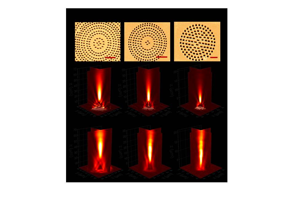
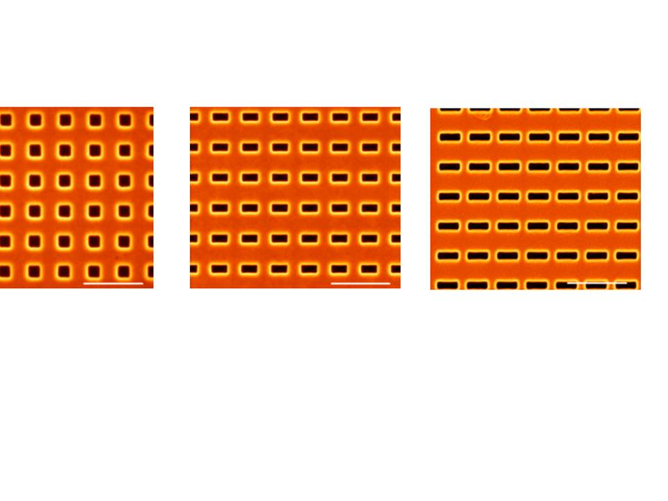
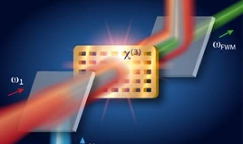
- The optical nonlinear response of plasmonic metasurfaces, and the use of modern fabrication technology to custom-design enhanced responses for specific spectroscopic purposes.
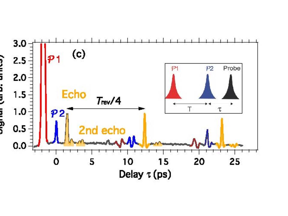
- Molecular alignment in response to femtosecond pulses, where we have introduced selectivity by means of properly designed pulse sequences and are currently studying echo phenomena.