Home page
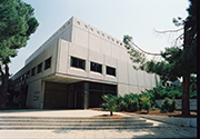
The Braun Center for Submicron Research, at the Weizmann Institute of Science, was founded in order to study and develop submicron semiconductor structures working in the mesoscopic regime. In the heart of this Center are three MBE laboratories with a task to develop and produce the purest and the most complex GaAs and InAs based semiconductors structures (heterostructures and nanowires). Nanostructure fabrication is provided by an electron beam writing (EBL) system, capable of producing less than 10 nm wide features. Two optical lithography laboratories enable patterning down to ~1 micrometer. UHV evaporators, UHV plasma etching and deposition tools, a SEM with less than 10 angstroms resolution, are some of the the fabrication tools. Low temperature measurements are done in dilution refrigerators, and in He4 and He3 systems. An optical laboratory of continuous and pulsed light allows optical characterization.