
Our lab is equipped with break junction setups at cryogenic temperatures. We employ a range of measurement techniques to analyze the structural and transport properties of atomic-scale conductors. In particular, we measure conductance, inelastic electron spectroscopy, shot noise, anisotropic and spin-valve magnetoresistance, and thermopower.
The Break Junction Technique
We employ the mechanically controllable break-junction (MCBJ) technique to form atomic and molecular junctions. A metal wire or thin strip with a central constriction is mounted on a flexible insulating substrate and placed in a vacuum chamber, where it is evacuated and cooled to 4.2 K. Controlled bending of the substrate breaks the wire, exposing two clean electrode apexes in cryogenic vacuum.
The inter-electrode separation can be controlled with picometer precision, enabling the formation of atomic junctions in which a single atom or a chain of atoms is suspended between the electrodes. Alternatively, molecules can be introduced to bridge the electrode apexes. Electron transport measurements over an ensemble of junction configurations are obtained by repeatedly breaking and reforming the junction.
Our break-junction setups are specifically designed for in situ chemical manipulation. They incorporate a heated molecular source that enables the introduction of purified molecules into the cryogenic junction. The in situ formation of atomic and molecular junctions at 4.2 K offers several key advantages: (1) the creation of ultra-clean electrode apexes with undercoordinated, highly reactive surface atoms (e.g., Ni, Pt, Al, Ag, Au); (2) elimination of solvents, thereby avoiding passivation or uncontrolled modifications of the electrode surfaces due to solvent molecules or contaminants; and (3) the flexibility to work with a wide range of molecules, including those that would decompose (e.g., oxygen) or chemically react with the undercoordinated atoms at the electrode tips to form metal-molecule hybrid systems that can be further controlled by changing the molecule orientation or atomic spacing.
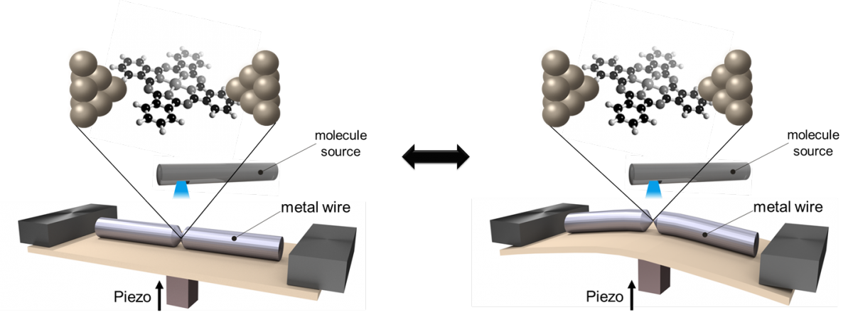
Schematic illustration of the break-junction technique. After breaking the metal wire, two clean electrode tips are formed in cryogenic vacuum. Molecules are introduced between the tips by in situ sublimation from a local source, and the tip separation can be tuned with sub-ångström precision.
Shot noise analysis
Current shot noise refers to time-dependent current fluctuations arising from the discrete nature of charge carriers. In nanoscale junctions, these fluctuations originate from the quantum-mechanical probabilities of electrons being transmitted through or reflected at the junction. Consequently, the noise depends on the conductance contributions of the individual transport channels within the junction, as described by the Landauer formalism. These conduction channels arise from the confinement of electron transport in the junction constriction, and their number in atomic-scale junctions is determined by the local electronic (orbital) structure. For example, electron transport in Au atomic junctions is typically carried by a single conduction channel dominated by the gold s valence orbital. In contrast, Ni atomic junctions exhibit multiple conduction channels due to the additional d valence orbitals that contribute to transport along the current direction.
Based on shot noise and conductance measurements, the number of conduction channels and their individual contributions can be determined. However, for systems with more than two channels, it is not possible to uniquely extract the exact conductance of each channel, as only two independent equations, for noise and total conductance, are available. To overcome this limitation, we relax the requirement for a unique solution and instead numerically determine the range of possible conductance contributions for each channel (R. Vardimon et al., Phys. Rev. B 88, 161404(R) (2013)). Despite the inherent uncertainty, this approach yields significant physical insight. For example, it enabled us to decompose conductance oscillations observed during the formation of Pt atomic chains into their channel components, revealing their orbital origin (R. Vardimon et al., Nano Lett. 14, 2988 (2014)). We further applied this method to study the evolution of spin-resolved conduction channels during the formation of nickel oxide atomic junctions (R. Vardimon et al., Nano Lett. 15, 3894 (2015)), and subsequently extended it to molecular junctions that exhibit spin-dependent quantum interference (A. N. Pal et al. Nature Commun. 10, 5565 (2019)).

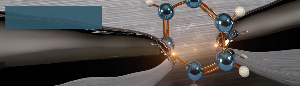
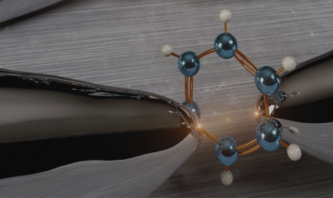
Schematics of an atomic-scale constriction in a conductor. When the diameter of the constriction approaches the electronic Fermi wavelength, the electrons are quantized in the transverse direction. As a result, only certain propagating electron modes (conduction channels) can be transmitted through the constriction.
Magnetoresistance measurements
Magnetoresistance is the change in electrical resistance under an applied magnetic field. Our sample design minimizes magneto-elastic motion of the electrodes. For spin-valve measurements, we use an asymmetric electrode geometry (Fig. 1c, inset) that enables parallel and antiparallel magnetization configurations. Our cryogenic systems include either a 9 T magnet or a 3–9 T vector magnet, providing both fixed-axis fields for spin-valve experiments and 360° rotating fields for anisotropic magnetoresistance measurements.
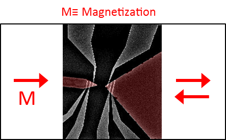
Asymmetric nickel electrodes (red) used for spin-valve experiments in atomic-scale junctions. The side electrodes (gray) enable independent monitoring of the magnetization of each electrode.