Ready for something new?
Dr. Omer Yaffe is on a quest for novel materials
New scientists

Like a student navigating the social and physical environment of a new school on the first day of class, electrons move about in materials in the same determined—yet somewhat discombobulated—manner.
A student will inadvertently enter the wrong classroom, scurry to a seat before all the good seats are taken, and make a new friend in the cafeteria, while an electron navigates through its environment, bumping, deflecting, scattering, and changing directions within materials.
The secret to understanding the electrical and structural properties of advanced new materials involves observing how electrons move from atom to atom and molecule to molecule. Scientists call this movement “electron transport,” and it is critical for evaluating the potential of new advanced materials.
Understanding this movement is central to the approach Dr. Omer Yaffe takes in studying so-called ‘soft’ semiconductors. Dr. Yaffe joined the Department of Materials and Interfaces in 2016, and is one of the new scientists working in the rapidly expanding field of new materials. Soft semiconductors lie at the forefront of this field.
Soft, flexible materials
Unlike conventional semiconductors, such as silicon, which are bound together by stable covalent or electron bonds, soft semiconductors are made of organic molecules, polymers, and ionic materials that are held together by weak atomic forces. Soft semiconductors are promising materials for the solar cells, electronic displays, and bright-light-emitting diodes of the future. Often transparent and flexible, they may be useful for future applications such as electronic skin, semi-transparent solar cells (for windows), and flexible electronics (e.g., for clothing). Soft semiconductors are also self-healing, may be inexpensive, can be processed in chemical solutions, and are readily deposited in large areas on a range of surfaces to create electronic components.
But one of the biggest challenges in the field remains: how to study their electron transport properties. Because these materials have a dynamic structure, conventional tools and models of electron transport are limited when studying them.
Dr. Yaffe is addressing that challenge by focusing on combining spectroscopy—how light interacts with matter—with measurements of electron transport to better understand the interplay between the structural dynamics and the electronic functions of soft semiconductors. This combination represents a foundational step in improving our understanding of soft semiconductor science, and could lead to the development of novel devices that are based on these relatively new materials.
“I want to understand the interplay between an electron and its environment, how a material responds to electron motion, and how that response in turn affects the electron,” says Dr. Yaffe.
Dr. Yaffe is an alumnus of the department he has joined. He completed his PhD here in 2012, where, under the guidance of Prof. David Cahen, he studied electron transport in hybrid organic-inorganic materials, and explored ways to “tune” the electronic properties of inorganic semiconductors for use in nanotechnology.
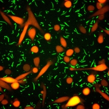
During his postdoctoral fellowship, he worked at the Columbia University Energy Frontier Research Center. There, he specialized in optical micro-spectroscopy and harnessed a method for detecting low-frequency atomic motion in soft materials. Using a specialized method called “THz-Domain Raman scattering”, he studied how a special kind of crystal called hybrid perovskite crystals rotate and vibrate. Hybrid perovskites have recently emerged as an excellent material for inexpensive, high-efficiency solar cells. Dr. Yaffe is continuing to investigate why they are so efficient for solar cell application, in order to design more materials.
He’s also capitalizing on recent advances in optical spectroscopy. Dr. Yaffe is developing a new spectroscopy method that allows him to map out the structural and electronic properties of organic/hybrid semiconductors, while also measuring electron transport. He plans to apply this approach to a variety of organic and hybrid semiconductor types, with an eye toward discovering how to design devices with improved electronics and performance.
Dr. Omer Yaffe is funded by the Benoziyo Fund for the Advancement of Science, the Larson Charitable Foundation, and Carolito Stiftung
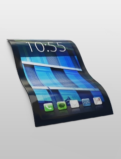
The bendable tablet is an example of a potential future application of the research of Dr. Omer Yaffe.