

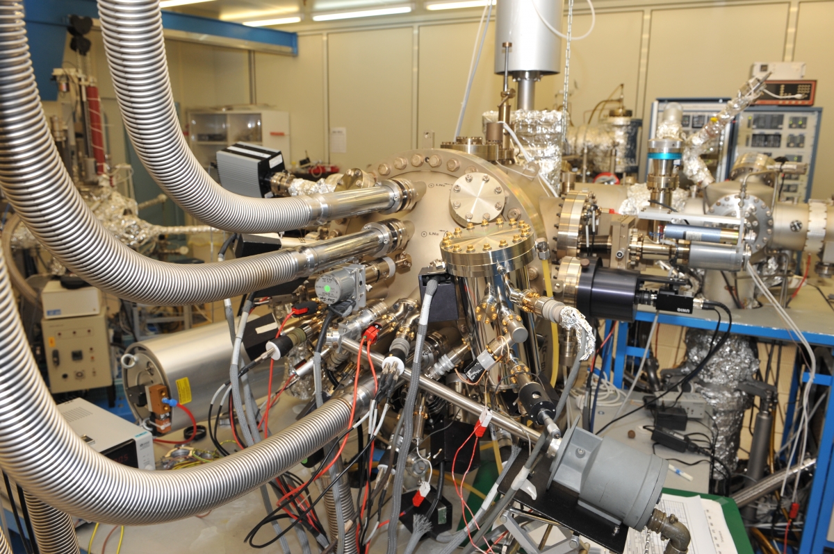
Molecular Beam Epitaxy (MBE)
The molecular beam epitaxy (MBE) laboratory is the heart of the submicron center. Its purpose is to prepare high purity semiconductor epitaxial layers (such as GaAs and AlGaAs). Two MBE systems at the submicron center includes two growth chambers in addition to six other for introduction and pre- treatment of the substrates. One growth chamber is designed to produce high purity materials (growing presently 2DEG with low temperature mobility 36x10^6cm^2/V-s) while the other growth chamber is growing semiconductor nano-wires (InAs and GaAs).

MBE for Nanowire growth
Previous MBE systems in the Braun Center was transformed to growth of semiconductor nanowires by the vapor-liquid-solid (VLS) technique. This activity concentrating mostly on growth of InAs and GaAs nanowires and heterostructure nanowires initially concentrated mostly on understanding and improving the crystalline structure and recently encompasses a range of mesoscopic physics studies, beginning with the Cooper pairs splitting experiment and observation of the Majorana fermions related zero bias peak.

E-beam
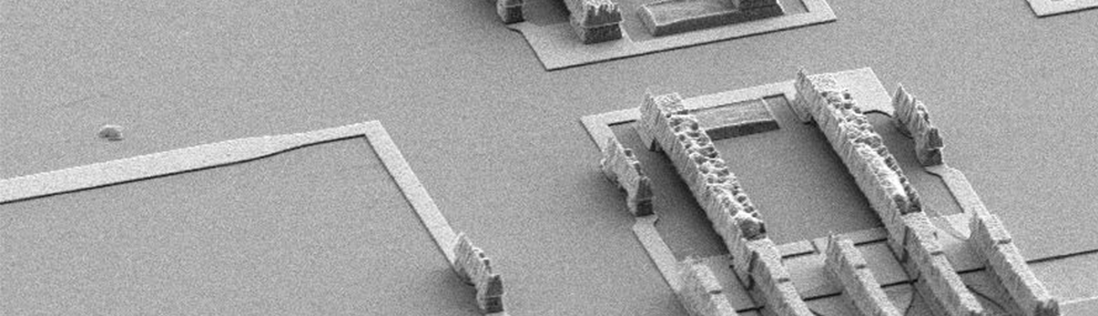
Submicron lithography is performed with a profession Electron Beam writing system. The E-Beam system is used to produce structures, via a well-focused electron beam that exposes an electron sensitive film, down to a minimum size of 5 nanometer. Layer stitching accuracy is ~10 nm. A profession 9300 JEOL system.

Optical Lithography
Connecting submicron structures to the ‘outside world’ is done via optical lithography of structures greater than about one micrometer. Exposing a layer of photoresist to blue light through an optical mask, which has the desired pattern printed on it, is used to define the structures. Subsequently, the semiconductor chips are etched (or metal deposited), through the reproduced photoresist mask. Three Karl Seiss systems, with the smallest possible exposed pattern ~0.6 micrometer.
