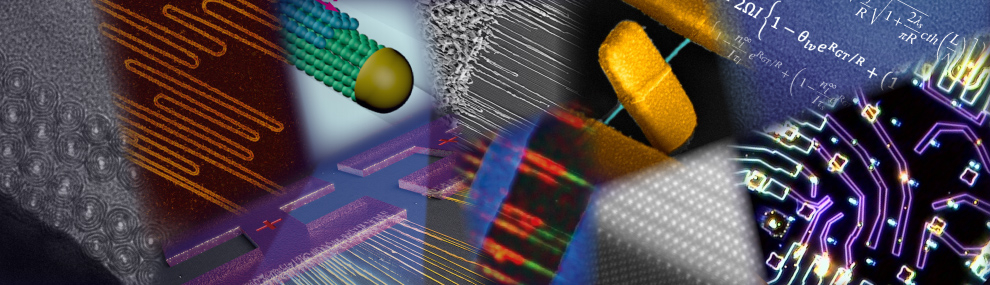
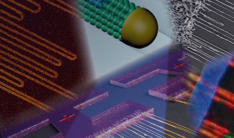
In nanostructures, as in macroscopic structures, shape and functionality are directly related to each other. For instance: a cross-bar architecture (where parallel an perpendicular lines cover a minimum area with a maximum number of crossings) can be the basis for a memory device; a serpentine shape (in which a single line covers gets closer to maximum number of point in a given area) is often used for cooling, heating, lighting or irrigation; a coil structure can be used to build electromagnets and dynamos. Nanostructures with such geomtries could likewise be the basis for nanosystems with analogous functions. But how to make them? Self-organization and guided growth can be used to generate these and other highly ordered complex structures at the nanoscale. Even the assembly of simpler geometries like parallel arrays of nanotubes, nanowires or nanoribbons with controlled position, direction and length is still a nontrivial and critical task for their integration into practical devices.
Our group investigates processes that lead to the formation of complex nanostructures. Some of these processes involve the growth of nanocrystals guided by surfaces (guided growth). Other processes involve the action of external forces such as electric fields or aerodynamic drag (directed self-assembly), or self-organization far from equilibrium.
Guided growth
During the last decade, we have reported the growth of perfectly aligned nanotubes, nanowires and nanowalls of various semiconductor materials with controlled crystallographic orientations on different substrates. The growth directions and crystallographic orientation of the nanowires are controlled by their epitaxial relationship with the substrate, as well as by a graphoepitaxial effect that guides their growth along surface steps and grooves. Four different modes of guided growth can thus be identified:
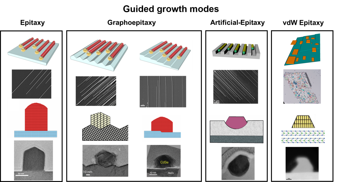
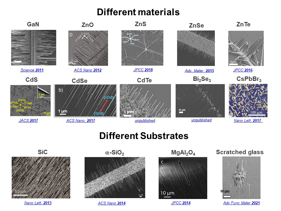
This guided growth approach was found to be very general and applicable to many materials and substrates:
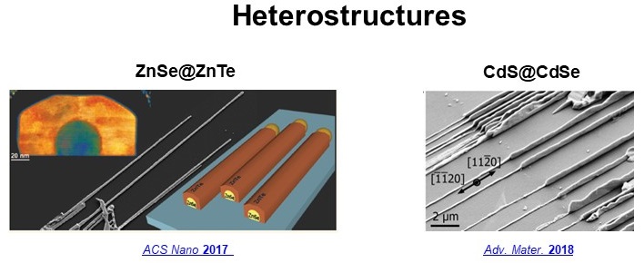
In addition to these single-material nanowires, we have produced guided heterostructures of two different semiconductors, including core-shell nanowires and nanowalls:
Using this guided growth approach, we achieved the massively parallel self-integration of nanowires into circuits and the production of optoelectronic nanosystems, including photodetectors, photodiodes and photovoltaic cells (see Functional nanosystems page).
Epitaxial mixed-dimensional nanostructures
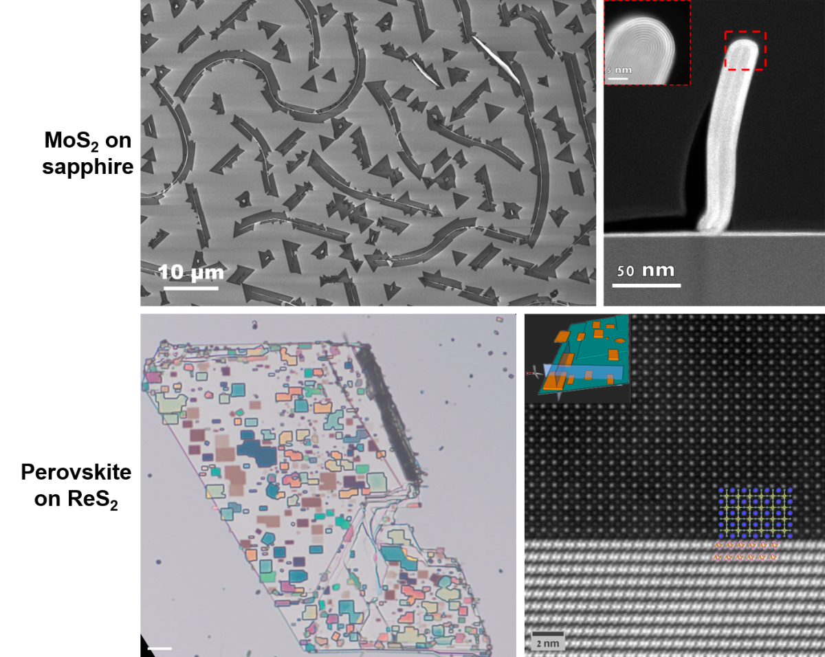
Mixed-dimensional heterostructures with unusual optoelectronic properties are created by placing two materials of different dimensionalities together, but often without control of their interface at the atomic level. Nanoribbons and nanofins combine in themselves the 2D character of their atomically thin constituents with the 1D character that arises from their elongated structure. They can have unique optoelectronic properties too, but are difficult to produce with well-defined geometries and to assemble into ordered arrays for integration into devices. We are currently extending our approach to create a variety of epitaxial mixed-dimensional nanostructures, including nanoribbons, nanofins and nanoplatelet-2D material heterostructures with a high degree of control at the atomic, nanoscopic and macroscopic levels, which enable their integration into devices.
Characterization
An important part of our research involves fundamental studies of the formation, structure and properties of the guided nanowires, such as their optical, electronic and optoelectronic properties. For these we use a vast array of methods (see our Lab page), including optical microscopy, SEM, AFM, TEM, Raman, CL, electrical and optoelectronic measurements. We also develop theoretical models to describe the formation mechanism, sometimes in collaboration with theorists.
We have developed a special setup for watching how guided nanowires grow in real time using in situ SEM. This allows us to take movies of growing nanowires like this one:
In addition, with these characterization methods used or developed in our lab and Weizmann facilities, we have carried out unique characterizations and measurements in collaboration with other groups. Below is a schematic representation of some of these methods.
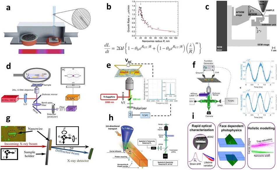 Schematic representation of unique analytical tools developed in our lab or in collaboration with other groups that are especially suited to the characterization of our nanomaterials and nanosystems: (a) Real-time imaging of surface-guided nanostructure formation by in situ, (b) kinetic analysis and modeling of nanostructure formation on surfaces, (c) in situ mechanical manipulation and force measurement by AFM inside a SEM, (d) optical mapping of crystallographic orientations by second-harmonic generation (SHG) polarimetry, optical determination of absolute polarity by SHG (e) and photoluminescence (PL) (f) under electric field, (g) scanning nanofocused XRD, (h) Spatially, temporally, and spectrally resolved PL microscopy characterization of energy and charge transport along nanowires, and (i) holistic high-throughput spectroscopy of large nanostructure ensembles.