
Publications
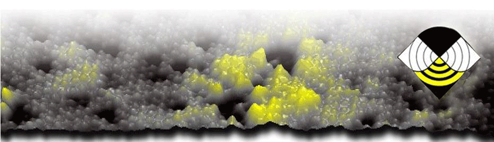
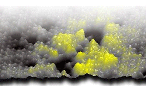
Strong electronic correlations often give rise to singular phenomena, such as strange metallicity, which appears in various quantum materials platforms. Understanding the mechanisms behind this universality remains an outstanding challenge, especially because the underlying degrees of freedom can be highly complex and varied. Flat-band systemsespecially kagome metalsprovide an ideal setting for investigating these properties. Here we demonstrate a pronounced zero-bias peakdip structure in the kagome metal Ni3In, in which the kagome flat band lies close to the Fermi energy. Scanning tunnelling spectroscopy reveals that the magnetic field and temperature evolution of these spectral features closely tracks the behaviour of the strange-metal state. We identify the origin of the zero-bias peak arising from compact molecular orbitals formed through destructive quantum interference across the kagome sites. This mechanism gives rise to emergent, f-shell-like localized moments within a d electron-based kagome metal, a manifestation of orbital-driven localization. Spectroscopic imaging further unveils the collapse of these quasiparticles across the Brillouin zone. Therefore, our findings provide insight into how different microscopic building blocks can become interconnected across seemingly disparate families of quantum materials and shed light on the universal nature of strange metallicity and correlated electron behaviour.
Following significant progress in the visualization and characterization of hybrid superconducting-semiconducting systems, greatly propelled by reports of Majorana zero modes in nanowire devices, considerable attention has been devoted to investigating the electronic structure at the buried superconducting-semiconducting interface and the nature of the induced superconducting correlations. The properties of that interface and the structure of the electronic wave functions that occupy it determine the functionality and the topological nature of the induced superconducting state. Here, we introduce a hybrid platform for proximity-inducing superconductivity in InAs0.6Sb0.4 nanowires, leveraging a unique architecture and material combination. By dispersing these nanowires over a superconducting indium film we exploit indium's high critical temperature of 3.7 K and the anticipated high spin-orbit and Zeeman couplings of InAs0.6Sb0.4. This design preserves the pristine top facet of the nanowires, making it highly compatible with scanning tunneling spectroscopy. Using this architecture we demonstrate that the mechanical contact supports Cooper-pair transparency as high as 90%, comparable with epitaxial interfaces. The anisotropic angular response to an applied magnetic field shows the quasi-two-dimensional nature of the parent superconductivity in the indium film and the quasi-one-dimensional nature of the induced superconductivity in the nanowires. Our platform offers robust and advantageous foundations for studying the emergence of topological superconductivity and the interplay of superconductivity and magnetism using atomic-scale spectroscopic tools.
Fe3GeTe2 has gained attention in the condensed matter community for its potential to be exfoliated into thin films with ferromagnetic (FM) order, thanks to its van der Waals layered structure and significant intrinsic anomalous Hall conductivity (AHC). In this work, we analyze the electronic structure and show that, contrary to prior claims, the bulk of the AHC cannot arise only from gapped nodal lines. By studying the materials symmetry properties, both with and without spin-orbit coupling (SOC) and across paramagnetic and FM phases, we find that Fe3GeTe2 hosts mirror-symmetry-protected nodal lines, which support surface drumhead states. Additionally, we identify three key sources of AHC: nodal lines in the paramagnetic phase gapped by the FM order, Weyl points within specific energy ranges, and gaps between spin-up and spin-down bands caused by SOC. Finally, our calculations suggest that electron doping could increase the AHC up to four times compared to its value at the computed Fermi level.
We demonstrate a topotactic transformation of zincblende InAs(Sb) nanowires into the Zintl phase Eu5In2As6 through a vapor-solid mutual exchange process involving Eu and In in molecular beam epitaxy. This conversion preserves the polyhedral coordination lattice of the parent InAs(Sb) structure while inducing orthorhombic symmetry in the product phase, Eu5In2As6, of which quasi-one-dimensional [InAs3]6- chains with tetrahedral sites align along the ⟨110⟩ direction of zincblende structure. Local and global magnetic characterization identified two distinct antiferromagnetic phase transitions at approximately 7 and 16 K in Eu5In2As6 nanowires, potentially classified as altermagnetic phases. The versatility of the topotactic conversion of III-V semiconductor nanowires provides a platform for designing functional Zintl materials with tunable magnetic properties, making them promising candidates for spintronic applications.
Most superconductors have an isotropic, single component order parameter and are well described by the standard (BCS) theory for superconductivity. Unconventional, multiple-component superconductors are exceptionally rare and are much less understood. Here, we combine scanning tunneling microscopy and angle-resolved macroscopic transport for studying the candidate chiral superconductor, 4Hb-TaS2. We reveal quasi-periodic one-dimensional modulations in the tunneling conductance accompanied by two-fold symmetric superconducting critical field. The strong modulation of the in-plane critical field, Hc2, points to a nematic, unconventional order parameter. However, the imaged vortex core is isotropic at low temperatures. We suggest a model that reconciles this apparent discrepancy and takes into account previously observed spontaneous time-reversal symmetry breaking at low temperatures. The model describes a competition between a dominating chiral superconducting order parameter and a nematic one. The latter emerges close to the normal phase. Our results strongly support the existence of two-component superconductivity in 4Hb-TaS2 and can provide valuable insights into other systems with coexistent charge order and superconductivity.
Due to quasi-one-dimensional confinement, nanowires possess unique electronic properties, which can promote specific device architectures. However, nanowire growth presents paramount challenges, limiting the accessible crystal structures and elemental compositions. Here we demonstrate solid-state topotactic exchange that converts wurtzite InAs nanowires into Zintl Eu3In2As4. Molecular-beam-epitaxy-based in situ evaporation of Eu and As onto InAs nanowires results in the mutual exchange of Eu from the shell and In from the core. Therefore, a single-phase Eu3In2As4 shell grows, which gradually consumes the InAs core. The mutual exchange is supported by the substructure of the As matrix, which is similar across the wurtzite InAs and Zintl Eu3In2As4 and therefore is topotactic. The Eu3In2As4 nanowires undergo an antiferromagnetic transition at a Néel temperature of ~6.5 K. Ab initio calculations confirm the antiferromagnetic ground state and classify Eu3In2As4 as a C2T axion insulator, hosting both chiral hinge modes and unpinned Dirac surface states. The topotactic mutual-exchange nanowire growth will, thus, enable the exploration of intricate magneto-topological states in Eu3In2As4 and potentially in other exotic compounds.
Coupling together distinct correlated and topologically nontrivial electronic phases of matter can potentially induce novel electronic orders and phase transitions among them. Transition metal dichalcogenide compounds serve as a bedrock for exploration of such hybrid systems. They host a variety of exotic electronic phases, and their Van der Waals nature enables to admix them, either by exfoliation and stacking or by stoichiometric growth, and thereby induce novel correlated complexes. Here, we investigate the compound 4Hb-TaS2 that interleaves the Mott-insulating state of 1T-TaS2 and the putative spin liquid it hosts together with the metallic state of 2H-TaS2 and the low-temperature superconducting phase it harbors using scanning tunneling spectroscopy. We reveal a thermodynamic phase diagram that hosts a first-order quantum phase transition between a correlated Kondo-like cluster state and a depleted flat band state. We demonstrate that this intrinsic transition can be induced by an electric field and temperature as well as by manipulation of the interlayer coupling with the probe tip, hence allowing to reversibly toggle between the Kondo-like cluster and the depleted flat band states. The phase transition is manifested by a discontinuous change of the complete electronic spectrum accompanied by hysteresis and low-frequency noise. We find that the shape of the transition line in the phase diagram is determined by the local compressibility and the entropy of the two electronic states. Our findings set such heterogeneous structures as an exciting platform for systematic investigation and manipulation of Mottmetal transitions and strongly correlated phases and quantum phase transitions therein.
Strong singularities in the electronic density of states amplify correlation effects and play a key role in determining the ordering instabilities in various materials. Recently high order van Hove singularities (VHSs) with diverging power-law scaling have been classified in single-band electron models. We show that the 110 surface of Bismuth exhibits high order VHS with an usually high density of states divergence ∼ (E)−0.7. Detailed mapping of the surface band structure using scanning tunneling microscopy and spectroscopy combined with first-principles calculations show that this singularity occurs in close proximity to Dirac bands located at the center of the surface Brillouin zone. The enhanced power-law divergence is shown to originate from the anisotropic flattening of the Dirac band just above the Dirac node. Such near-coexistence of massless Dirac electrons and ultra-massive saddle points enables to study the interplay of high order VHS and Dirac fermions.
Confining two dimensional Dirac fermions on the surface of topological insulators has remained an outstanding conceptual challenge. Here we show that Dirac fermion confinement is achievable in topological crystalline insulators (TCI), which host multiple surface Dirac cones depending on the surface termination and the symmetries it preserves. This confinement is most dramatically reflected in the flux dependence of these Dirac states in the nanowire geometry, where different facets connect to form a closed surface. Using SnTe as a case study, we show how wires with all four facets of the (100) type display novel Aharonov-Bohm oscillations, while nanowires with the four facets of the (110) type such oscillations are absent due to strong confinement of the Dirac states to each facet separately. Our results place TCI nanowires as a versatile platform for confining and manipulating Dirac surface states.
In the pursuit of magneto-electronic systems nonstoichiometric magnetic elements commonly introduce disorder and enhance magnetic scattering. We demonstrate the growth of (EuIn)As shells, with a unique crystal structure comprised of a dense net of Eu inversion planes, over InAs and InAs1-xSbxcore nanowires. This is imaged with atomic and elemental resolution which reveal a prismatic configuration of the Eu planes. The results are supported by molecular dynamics simulations. Local magnetic and susceptibility mappings show magnetic response in all nanowires, while a subset bearing a DC signal points to ferromagnetic order. These provide a mechanism for enhancing Zeeman responses, operational at zero applied magnetic field. Such properties suggest that the obtained structures can serve as a preferred platform for time-reversal symmetry broken one-dimensional states including intrinsic topological superconductivity.
Magnetic topological materials represent a class of compounds with properties that are strongly influenced by the topology of their electronic wave functions coupled with the magnetic spin configuration. Such materials can support chiral electronic channels of perfect conduction, and can be used for an array of applications, from information storage and control to dissipationless spin and charge transport. Here we review the theoretical and experimental progress achieved in the field of magnetic topological materials, beginning with the theoretical prediction of the quantum anomalous Hall effect without Landau levels, and leading to the recent discoveries of magnetic Weyl semimetals and antiferromagnetic topological insulators. We outline recent theoretical progress that has resulted in the tabulation of, for the first time, all magnetic symmetry group representations and topology. We describe several experiments realizing Chern insulators, Weyl and Dirac magnetic semimetals, and an array of axionic and higher-order topological phases of matter, and we survey future perspectives.
The physical realization of Chern insulators is of fundamental and practical interest, as they are predicted to host the quantum anomalous Hall (QAH) effect and topologically protected chiral edge states which can carry dissipationless current. Current realizations of the QAH state often require complex heterostructures and sub-Kelvin temperatures, making the discovery of intrinsic, high temperature QAH systems of significant interest. In this work we show that time-reversal symmetry breaking Weyl semimetals, being essentially stacks of Chern insulators with inter-layer coupling, may provide a new platform for the higher temperature realization of robust chiral edge states. We present combined scanning tunneling spectroscopy and theoretical investigations of the magnetic Weyl semimetal, Co3Sn2S2. Using modeling and numerical simulations we find that depending on the strength of the interlayer coupling, chiral edge states can be localized on partially exposed kagome planes on the surfaces of a Weyl semimetal. Correspondingly, our dI/dV maps on the kagome Co3Sn terraces show topological states confined to the edges which display linear dispersion. This work provides a new paradigm for realizing chiral edge modes and provides a pathway for the realization of higher temperature QAH effect in magnetic Weyl systems in the two-dimensional limit.
Topological superconductors are an essential component for topologically protected quantum computation and information processing. Although signatures of topological superconductivity have been reported in heterostructures, material realizations of intrinsic topological superconductors are rather rare. Here we use scanning tunnelling spectroscopy to study the transition metal dichalcogenide 4Hb-TaS2 that interleaves superconducting 1H-TaS2 layers with strongly correlated 1T-TaS2 layers, and find spectroscopic evidence for the existence of topological surface superconductivity. These include edge modes running along the 1H-layer terminations as well as under the 1T-layer terminations, where they separate between superconducting regions of distinct topological nature. We also observe signatures of zero-bias states in vortex cores. All the boundary modes exhibit crystallographic anisotropy, whichtogether with a finite in-gap density of states throughout the 1H layersallude to the presence of a topological nodal-point superconducting state. Our theoretical modelling attributes this phenomenology to an inter-orbital pairing channel that necessitates the combination of surface mirror symmetry breaking and strong interactions. It, thus, suggests a topological superconducting state realized in a natural compound.
The cross-sectional dimensions of nanowires set the quantization conditions for the electronic subbands they host. These can be used as a platform to realize one-dimesional topological superconductivity. Here we develop a protocol that forces such nanowires to kink and change their growth direction. Consequently, a thin rectangular nanoplate is formed, which gradually converges into a very thin square tip. We characterize the resulting tapered nanowires structurally and spectroscopically by scanning and transmission electron microscopy and scanning tunneling microscopy and spectroscopy and model their growth. A unique structure composed of ordered rows of atoms on the (110) facet of the nanoflag is further revealed by atomically resolved topography and modeled by simulations. We discuss possible advantages tapered InAs nanowires offer for Majorana zero-mode realization and manipulation.
Dual topological materials are unique topological phases that host coexisting surface states of different topological nature on the same or on different material facets. Here, we show that Bi
2TeI is a dual topological insulator. It exhibits band inversions at two time reversal symmetry points of the bulk band, which classify it as a weak topological insulator with metallic states on its side surfaces. The mirror symmetry of the crystal structure concurrently classifies it as a topological crystalline insulator. We investigated Bi
2TeI spectroscopically to show the existence of both two-dimensional Dirac surface states, which are susceptible to mirror symmetry breaking, and one-dimensional channels that reside along the step edges. Their mutual coexistence on the step edge, where both facets join, is facilitated by momentum and energy segregation. Our observation of a dual topological insulator should stimulate investigations of other dual topology classes with distinct surface manifestations coexisting at their boundaries.
Following significant progress in the visualization and characterization of Majorana end modes in hybrid systems of semiconducting nanowires and superconducting islands, much attention is devoted to the investigation of the electronic structure at the buried interface between the semiconductor and the superconductor. The properties of that interface and the structure of the electronic wave functions that occupy it determine the functionality and the topological nature of the superconducting state induced therein. Here we study this buried interface by performing spectroscopic mappings of superconducting aluminum islands epitaxially grown in situ on indium arsenide nanowires. We find unexpected robustness of the hybrid system as the direct contact with the aluminum islands does not lead to any change in the chemical potential of the nanowires, nor does it induce a significant band bending in their vicinity. We attribute this to the presence of surface states bound to the facets of the nanowire. Such surface states, which are present also in bare nanowires prior to aluminum deposition, pin the Fermi level, thus rendering the nanowires resilient to surface perturbations. The aluminum islands further display Coulomb blockade gaps and peaks that signify the formation of a resistive tunneling barrier at the InAs-Al interface. The extracted interface resistivity, ρ≈1.3×10⁻⁶ ω cm2, will allow us to proximity induce superconductivity with negligible Coulomb blockade effects by islands with interface area as small as 0.01 μm2. At low energies we identify a potential energy barrier that further suppresses the transmittance through the interface. A corresponding barrier exists in bare semiconductors between surface states and the accumulation layer, induced to maintain charge neutrality. Our observations elucidate the delicate interplay between the resistive nature of the InAs-Al interface and the ability to proximitize superconductivity and tune the chemical potential in semiconductor-superconductor hybrid nanowires.
Nonzero weak topological indices are thought to be a necessary condition to bind a single helical mode to lattice dislocations. In this work we show that higher-order topological insulators (HOTIs) can, in fact, host a single helical mode along screw or edge dislocations (including step edges) in the absence of weak topological indices. When this occurs, the helical mode is necessarily bound to a dislocation characterized by a fractional Burgers vector, macroscopically detected by the existence of a stacking fault. The robustness of a helical mode on a partial defect is demonstrated by an adiabatic transformation that restores translation symmetry in the stacking fault. We present two examples of HOTIs, one intrinsic and one extrinsic, that show helical modes at partial dislocations. Since partial defects and stacking faults are commonplace in bulk crystals, the existence of such helical modes can measurably affect the expected conductivity in these materials.
The growing diversity of topological classes leads to ambiguity between classes that share similar boundary phenomenology. This is the status of bulk bismuth. Recent studies have classified it as either a strong or a higher-order topological insulator, both of which host helical modes on their boundaries. We resolve the topological classification of bismuth by spectroscopically mapping the response of its boundary modes to a screw-dislocation. We find that the one-dimensional mode, on step-edges, extends over a wide energy range and does not open a gap near the screw-dislocations. This signifies that this mode binds to the screw-dislocation, as expected for a material with nonzero weak indices. We argue that the small energy gap, at the time reversal invariant momentum L, positions bismuth within the critical region of a topological phase transition between a higher-order topological insulator and a strong topological insulator with nonzero weak indices.
Bulk-surface correspondence in Weyl semimetals ensures the formation of topological " Fermi arc" surface bands whose existence is guaranteed by bulk Weyl nodes. By investigating three distinct surface terminations of the ferromagnetic semimetal Co3Sn2S2, we verify spectroscopically its classification as a time-reversal symmetry-broken Weyl semimetal. We show that the distinct surface potentials imposed by three different terminations modify the Fermi-arc contour and Weyl node connectivity. On the tin (Sn) surface, we identify intra-Brillouin zone Weyl node connectivity of Fermi arcs, whereas on cobalt (Co) termination, the connectivity is across adjacent Brillouin zones. On the sulfur (S) surface, Fermi arcs overlap with nontopological bulk and surface states. We thus resolve both topologically protected and nonprotected electronic properties of a Weyl semimetal.
We draw a phenomenological analogy between the topological defect of a screw dislocation and the electronic Weyl semimetal topology class including their bulk and surface manifestations. In the bulk, both can be assigned a chirality which can be calculated from the crystallographic curvature of the screw dislocation or the Berry curvature of the Weyl bands. On the surface, the chiral screw dislocations give rise to open-contour surface modes in the form of a crystallographic step edge uniquely emanating from the screw termination. The bulk Weyl nodes induce surface Fermi-arc states that uniquely terminate at the surface projection of the bulk Weyl node. We use scanning tunneling microscopy to visualize the surface manifestation of both topological structures. The surface topology of the screw dislocation is visualized in the surface topography. The surface momentum-space topology of the Weyl semimetal is visualized and characterized spectroscopically using quasi-particle interference.
Exotic electronic states are realized in novel quantum materials. This field is revolutionized by the topological classification of materials. Such compounds necessarily host unique states on their boundaries. Scanning tunneling microscopy studies of these surface states have provided a wealth of spectroscopic characterization, with the successful cooperation of ab initio calculations. The method of quasiparticle interference imaging proves to be particularly useful for probing the dispersion relation of the surface bands. Herein, how a variety of additional fundamental electronic properties can be probed via this method is reviewed. It is demonstrated how quasiparticle interference measurements entail mesoscopic size quantization and the electronic phase coherence in semiconducting nanowires; helical spin protection and energy-momentum fluctuations in a topological insulator; and the structure of the Bloch wave function and the relative insusceptibility of topological electronic states to surface potential in a topological Weyl semimetal.
We study the role of gold droplets in the initial stage of nanowire growth via the vapor-liquid-solid method. Apart from serving as a collections center for growth species, the gold droplets carry an additional crucial role that necessarily precedes the nanowire emergence, that is, they assist the nucleation of nanocraters with strongly faceted {111}B side walls. Only once these facets become sufficiently large and regular, the gold droplets start nucleating and guiding the growth of nanowires. We show that this dual role of the gold droplets can be detected and monitored by high-energy electron diffraction during growth. Moreover, gold induced formation of craters and the onset of nanowires growth on the {111}B facets inside the craters are confirmed by the results of Monte Carlo simulations. The detailed insight into the growth mechanism of inclined nanowires will help to engineer new and complex nanowire-based device architectures.
It was recently shown that in situ epitaxial aluminum coating of indium arsenide nanowires is possible and yields superior properties relative to ex-situ evaporation of aluminum (Nat. Mater. 2015, 14, 400-406). We demonstrate a robust and adaptive epitaxial growth protocol satisfying the need for producing an intimate contact between the aluminum superconductor and the indium arsenide nanowire. We show that the (001) indium arsenide substrate allows successful aluminum side-coating of reclined indium arsenide nanowires that emerge from (111)B microfacets. A robust, induced hard superconducting gap in the obtained indium arsenide/aluminum core/partial shell nanowires is clearly demonstrated. We compare epitaxial side-coating of round and hexagonal cross-section nanowires and find the surface roughness of the round nanowires to induce a more uniform aluminum profile. Consequently, the extended aluminum grains result in increased strain at the interface with the indium arsenide nanowire, which is found to induce dislocations penetrating into round nanowires only. A unique feature of proposed growth protocol is that it supports in situ epitaxial deposition of aluminum on all three arms of indium arsenide nanowire intersections in a single growth step. Such aluminum coated intersections play a key role in engineering topologically superconducting networks required for Majorana based quantum computation schemes.
The higher the energy of a particle is above equilibrium, the faster it relaxes because of the growing phase space of available electronic states it can interact with. In the relaxation process, phase coherence is lost, thus limiting high-energy quantum control and manipulation. In one-dimensional systems, high relaxation rates are expected to destabilize electronic quasiparticles. Here, we show that the decoherence induced by relaxation of hot electrons in one-dimensional semiconducting nanowires evolves nonmonotonically with energy such that above a certain threshold hot electrons regain stability with increasing energy. We directly observe this phenomenon by visualizing, for the first time, the interference patterns of the quasi-one-dimensional electrons using scanning tunneling microscopy. We visualize the phase coherence length of the one-dimensional electrons, as well as their phase coherence time, captured by crystallographic Fabry-Pèrot resonators. A remarkable agreement with a theoretical model reveals that the nonmonotonic behavior is driven by the unique manner in which one-dimensional hot electrons interact with the cold electrons occupying the Fermi sea. This newly discovered relaxation profile suggests a high-energy regime for operating quantum applications that necessitate extended coherence or long thermalization times, and may stabilize electronic quasiparticles in one dimension.
We introduce a coupled-layer construction to describe three-dimensional topological crystalline insulators protected by reflection symmetry. Our approach uses stacks of weakly coupled two-dimensional Chern insulators to produce topological crystalline insulators in one higher dimension, with tunable number and location of surface Dirac cones. As an application of our formalism, we turn to a simplified model of topological crystalline insulator SnTe, showing that its protected surface states can be described using the coupled-layer construction.
Fermi arcs are the surface manifestation of the topological nature of Weyl semimetals, enforced by the bulk-boundary correspondence with the bulk Weyl nodes. The surface of tantalum arsenide, similar to that of other members of the Weyl semimetal class, hosts nontopological bands that obscure the exploration of this correspondence. We use the spatial structure of the Fermi arc wave function, probed by scanning tunneling microscopy, as a spectroscopic tool to distinguish and characterize the surface Fermi arc bands. We find that, as opposed to nontopological states, the Fermi arc wave function is weakly affected by the surface potential: it spreads rather uniformly within the unit cell and penetrates deeper into the bulk. Fermi arcs reside predominantly on tantalum sites, from which the topological bulk bands are derived. Furthermore, we identify a correspondence between the Fermi arc dispersion and the energy and momentum of the bulk Weyl nodes that classify this material as topological. We obtain these results by introducing an analysis based on the role the Bloch wave function has in shaping quantum electronic interference patterns. It thus carries broader applicability to the study of other electronic systems and other physical processes.
We study the distribution of transport current across superconducting Bi2 Sr2 CaCu2 O8 crystals and the vortex flow through the sample edges. We show that the Tx transition is of electrodynamic rather than thermodynamic nature, below which vortex dynamics is governed by the edge inductance instead of the resistance. This allows measurement of the resistance down to 2 orders of magnitude below the transport noise. By irradiating the current contacts the resistive step at vortex melting is shown to be due to loss of c -axis correlations rather than breakdown of quasilong-range order within the a-b planes.
A low concentration of columnar defects is reported to transform a first-order vortex lattice melting line in Bi2Sr2CaCu2O8 crystals into alternating segments of first- and second-order transitions separated by two critical points. As the density of columnar defects is increased, the critical points shift apart and the range of the intermediate second-order transition expands. The measurement of equilibrium magnetization and the mapping of the melting line down to 27 K was made possible by employment of the shaking technique.
We study the oxygen doping dependence of the equilibrium first-order melting and second-order glass transitions of vortices in Bi2Sr2CaCu2O8+δ. Doping affects both anisotropy and disorder. Anisotropy scaling is shown to collapse the melting lines only where thermal fluctuations are dominant. Yet, in the region where disorder breaks that scaling, the glass lines are still collapsed. A quantitative fit to melting and replica symmetry-breaking lines of a 2D Ginzburg-Landau model further reveals that disorder amplitude weakens with doping, but to a lesser degree than thermal fluctuations, enhancing the relative role of disorder.
The thermodynamic H-T phase diagram of Bi2Sr2CaCu2O8 was mapped by measuring local equilibrium magnetization M(H,T) in the presence of vortex shaking. Two equally sharp first-order magnetization steps are revealed in a single temperature sweep, manifesting a liquid-solid-liquid sequence. In addition, a second-order glass transition line is revealed by a sharp break in the equilibrium M(T) slope. The first- and second-order lines intersect at intermediate temperatures, suggesting the existence of four phases: Bragg glass and vortex crystal at low fields, glass and liquid at higher fields.