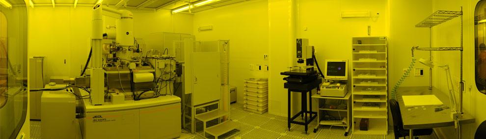

Electron Beam Lithography Laboratory
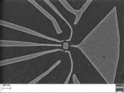
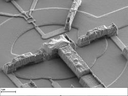
Processing of state of the art ultra small structures which include submicron active areas, air briges and T- gates produced on III-V materials by Electron beam lithography (EBL). EBL is used for research into the scaling limits of integrated circuits and studies of quantum effects and other novel physics phenomena at very small dimensions.
A typical application is the study of the Aharanov-Bohm effect, where electrons traveling along two different paths about a micrometer in length can interfere constructively or destructively, depending on the strength of an applied magnetic field. Other applications include devices to study ballistic electron effects, quantization of electron energy levels in very small structures, and single electron transistors. To see these effects typically requires minimum feature sizes of 20 nm or less, as well as operation at cryogenic temperatures.