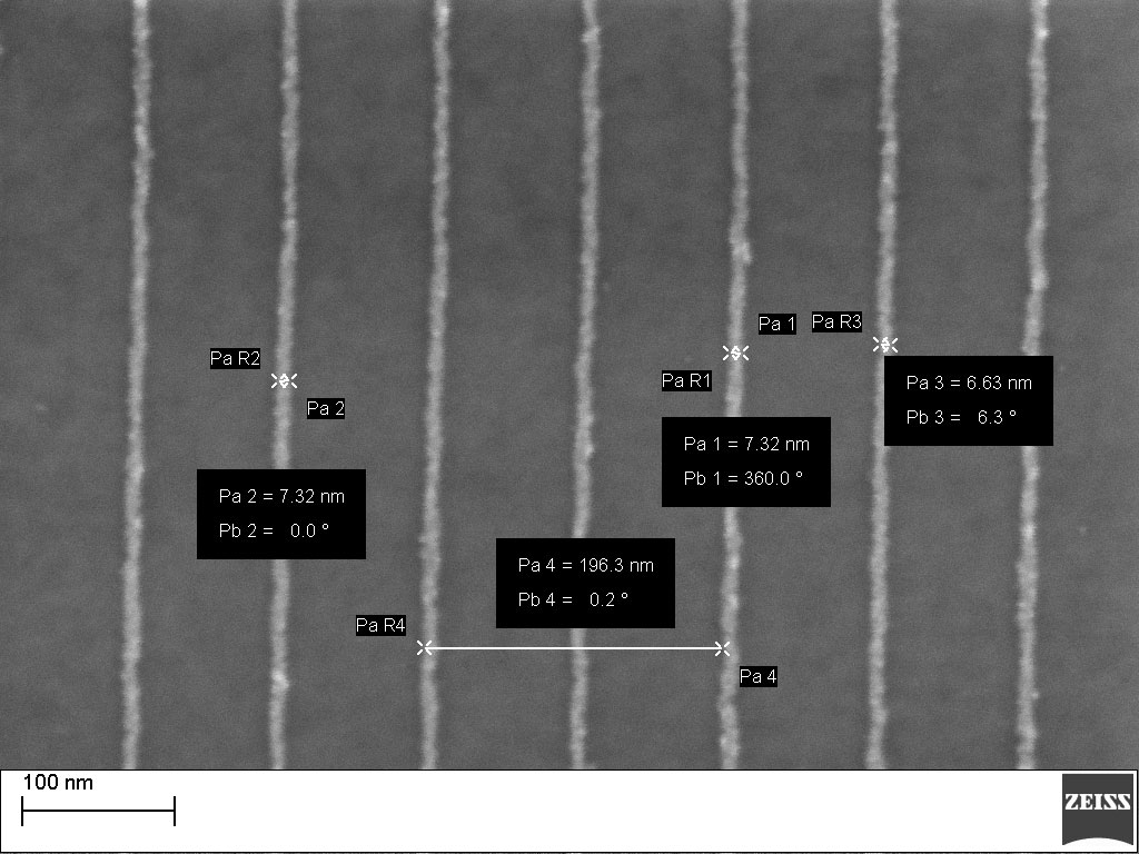
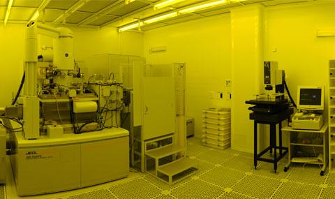
Typical processes include bi- layer resists at different resist sensitivities that are exposed selectively using appropriate exposure doses. These exposures interact with each other, and are obscured by electron scattering, thus high resolution PEC, and cold developing techniques need to be applied.


