Images of Selected Nano-Systems
Figure 1: Molecular-Beam Epitaxy (MBE)
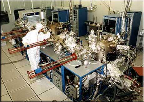 |
| MBE growth/analysis system at the Braun Submicron Center at the Weizmann Institute inside a ultra-high vacuum chamber growing epitaxial layers (such as Gallium Arsenide and Aluminum Gallium Arsenide) one by one with excellent control over materials and purity. Such grown layers (using MBE, or often less exacting methods) form the basis of manysemiconductor devices. |
Figure 2a: Exploiting Tunneling: the Scanning Tunneling Microscope (STM)
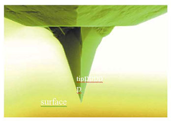 An atomic force microscope (AFM) tip An atomic force microscope (AFM) tip |
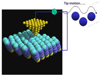 A 3D rendering of the STM setup A 3D rendering of the STM setup |
Figure 2b: STM in Action: the positioning of Xe atoms on the surface of copper (M. Crommie & D. Eigler)
 The process of Pick and Place Atoms |
Figure 3: Feynmann, and Excerpts from his 1959 Lecture
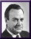
Richard P. Feynmann, 1918-1988
One of the greatest physicists of the 20th century
See biographical data.
In addition to his decisive contributions to, for example, the path-integral picture of quantum mechanics, his ingenious theory of superfluid helium, the breakthrough in quantum electrodynamics and other problems associated with quantum fields, he also made important contributions to the Physics discussed here. We cite the Feynmann-Vernon theory of how the coupling to the environment weakens the quantum mechanical effects. An excerpt from his December 29th, 1959 public lecture is reproduced below. It can be read in its entirety and downloaded from http://www.zyvex.com/nanotech/feynman.html.
There's Plenty of Room at the Bottom
An invitation to enter a new field of Physics
I would like to describe a field, in which little has been done, but in which an enormous amount can be done in principle. This field is not quite the same as the others in that it will not tell us much of fundamental physics (in the sense of, "What are the strange particles?") but it is more like solid-state physics in the sense that it might tell us much of great interest about the strange phenomena that occur in complex situations. Furthermore, a point that is most important is that it would have an enormous number of technical applications.
What I want to talk about is the problem of manipulating and controlling things on a small scale.
...As soon as I mention this, people tell me about miniaturization, and how far it has progressed today. They tell me about electric motors that are the size of the nail on your small finger. And there is a device on the market, they tell me, by which you can write the Lord's Prayer on the head of a pin. But that's nothing; that's the most primitive, halting step in the direction I intend to discuss. It is a staggeringly small world that is below. In the year 2000, when they look back at this age, they will wonder why it was not until the year 1960 that anybody began seriously to move in this direction.
Why cannot we write the entire 24 volumes of the Encyclopedia Britannica on the head of a pin?
We leave it to the reader to ponder how close have we reached in the year 2000, in fulfilling this last expectation by Feynmann. He once said "all of quantum mechanics is contained in the two slit experiment, unfortunately no one understands the two slit experiment." How Feynmann would humorously depict the famous experiment with particles, is shown below. Remarkably, one of his insights has proven to be useful for modern state-of-the-art research: http://www.colorado.edu/physics/2000/schroedinger/two-slit3.html.

Feynmann: armor for slit and brick or wood for the absorber
Figure 4: Local Compressibility of the 2D electron gas (S. Ilani, et al. 2001)
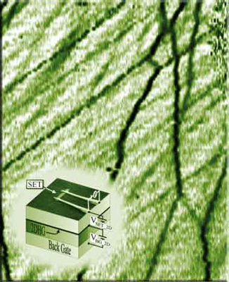 |
| Measurement of discrete charging events in a low densities two dimensional hole gas, which fragments on the nanoscale into microscopic charge configurations that coexist with the surrounding metallic compressible phase. The black lines in the figure are the individual charging events of these fragments. The mutual electrostatic interactions between them are manifested by the vertices formed at their crossings. Inset: The measurement circuit that utilizes a single electron transistor as a local detector of compressibility. The color map represents inverse electronic compressibility. |
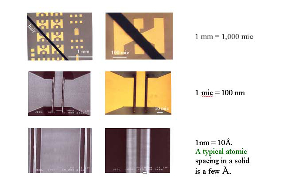
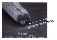
Figure 5: Size scales
|
1mm → 100 micron → 10 micron → 1 micron → 100nm. Detail in lower right part of the last image is a small state-of-the art-transistor, compared with a commercially available one in 2001. (Courtesy of D. Mahalu and M. Heiblum) |
 |
 And where do we go from here? And where do we go from here? |
Figure 6: DNA molecules bridging two metallic electrodes

| Figure 7: The Quantum Hall effect (QHE), von Klitzing et. al. (1982) | |
 (a) Concept of Hall effect (a) Concept of Hall effect |
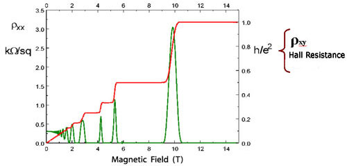 (b) Results for QHE (b) Results for QHE |
Figure 8: Point-contact Conductance
| (a) Quantization of Pt-contact Conductance | (b) Pt-contact conductance and shot-noise |
 Two-terminal point-contact conductance vs. gate voltage, for several magnetic fields at 0.6K (van Wees et al.) Two-terminal point-contact conductance vs. gate voltage, for several magnetic fields at 0.6K (van Wees et al.) |
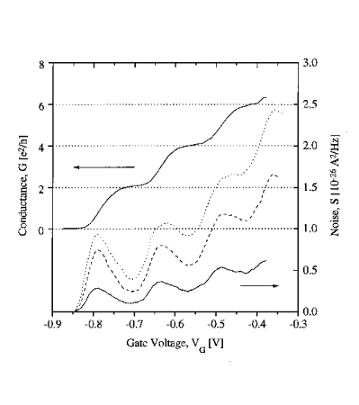 The conductance of a QPC in a 2D electron gas as a function of gate voltage, from Reznikov et al. The RHS scale is for the lower curves giving the shot-noise power at various transport votages. The conductance of a QPC in a 2D electron gas as a function of gate voltage, from Reznikov et al. The RHS scale is for the lower curves giving the shot-noise power at various transport votages. |
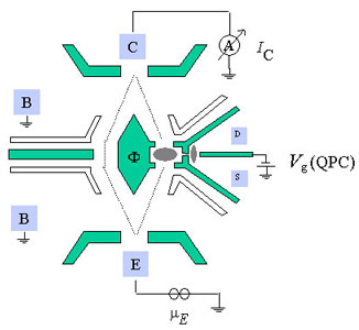
Figure 9: Concept of Mesoscopic A-B Interferometer
| Electronic, Solid-state! Electrons confined by real wires | |
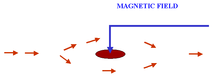 Wave Comes from the left, splits to two paths which encircle the A-B Magnetic Field (thick, blue line) and combine at the output The current is proportional to the voltage and is periodic in the flux. Ideally, the magnetic field is zero, or its effect is negligible, in the wires confining the electrons. |
|
Figure 10: A-B Oscillations in Au rings (Webb, et al.)
| Aharonov-Bohm Effect in Normal Metals | |
 |
|
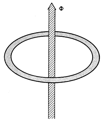
Figure 11: A-B Flux in an isolated ring
| Persistent equilibrium currents exist for finite Φ | |
 |
|
| Figure 12: Persistent Currents experiment | |
 |
 |
|
Ring structures built with high quality semiconductor 2DEG microtechnogy (Mailly, et al.), using gates to connect and disconnect the ring to electrical contacts. A special SQUID was used to measure the magnetiuc monent produced by the current. The graph shows the Fourier components of the current vs flux, peaking at h/e and its harmonics. This is a demonstration of persistent currents. |
|
Figure 13: The "Coulomb Blockade"
 |
|
The Coulomb blockade phenomenon as observed by Buks et al, in the context of controlled dephasing (Figs. 15 and 16), for a "quantum dot" (QD) bridging two conducting lines. The "plunger voltage" changes the potential energy of the dot. When its discrete quantum levels are brought one by one into resonance with the Fermi lavels of the lines. When this happens, a peak of the differential with height approaching GQ follows (top graph) and the total electron number on the QD increases by one (middle graph). The QD electrostatic potential (lower graph) is steadily and linearly decreased, but jumps by e2/2C across each charging event. The Coulomb staircase is the total current when the source-drain (transport) voltage is increased. It resembles the middle graph. |
Figure 14: One-dimensional transistor structures based on a nanotube gated from below and conducting electrodes: (upper) by C. Dekker, et al., and (lower) by P. Avouris, et al.
| A logic gate consisting of an n-type FET and a p-type one, in series. | |
 |
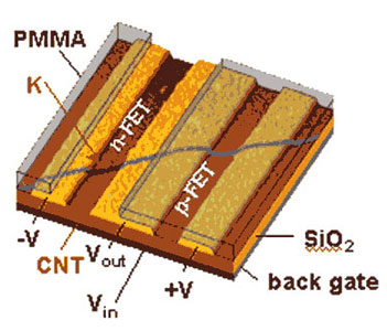 |
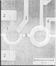
Figure 15: Sample for the controlled dephasing experiment
| Schematic | SEM picture of real device used by Buks et al. |
 |
 |
Figure 16: Conotrolled dephasing of AB oscillations (Buks et al.)
 Visibilty  of A-B oscillations reduced when QPT current increases. of A-B oscillations reduced when QPT current increases. |
Figure 17: Nanotubes, artist's concept and real Image (C. Dekker et al.)
 Computer view Computer view |
 STM imaging STM imaging |
Figure 18: Various types of Nanotubes, obtained by rolling and gluing the graphene sheet, as shown.
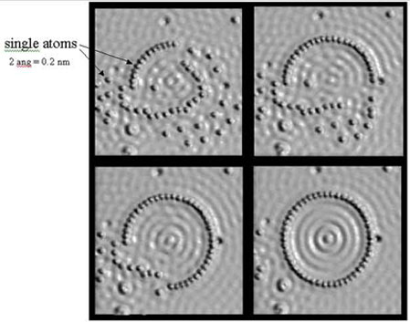
Figure 19: "Kondo Mirage, D. Eigler et al., IBM Almaden
  |
|
Images of man-made elliptic arrangements of atoms on a metallic surface, both prepared and visualized, using an STM system. In addition to the boundaries of the atomic "corral", a specific magnetic impurity was deposited at desired points inside the latter. These and others are described in: http://www.almaden.ibm.com/almaden/media/image_mirage.html. Some unusual Physical phenomena due to the wave nature of the electrons and their correlations around the impurity were demonstrated in experiments using these samples: Placing the impurity just at a focal point of the ellipse, created a shadow (a "mirage") in the other focus. |