MBE structures for nano-devices
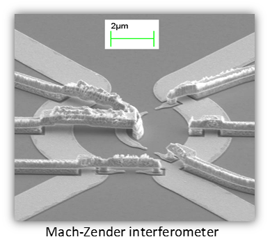
In a high mobility 2DEG, the electrons’ elastic mean free path may significantly exceed the physical size of small devices. In quantum systems, electron wave behavior prevails, and transport properties must be assessed by calculating transmission amplitudes rather than the microscopic conductivity. Ubiquitous devices are built by fabricating metal gates on the surface to the heterostructure hosting the 2DEG, which are able to deplete a 2DEG underneath; thus, nano-scale conducting regions can be created in the plane of the 2DEG. Among them quantum dots, quantum point contacts, quantum wires, interferometers, etc. Various physical effects, e.g., Coulomb blockade, Aharonov-Bohm interference, current fluctuations, and others associated with ballistic transport, have been extensively studied using this platform during past 20 years.
Nowadays, such devices became indispensable tools in the field of quantum Hall physics, allowing studying exotic Hall states using interferometric techniques, shot-noise measurements, etc. The major challenge in the design of the structure and the MBE growth, aside from the high electron mobility, is the temporal stability of the device, which can be achieved by careful band gap engineering and the application of proper doping schemes.
2DEG for Quantum Hall Physics
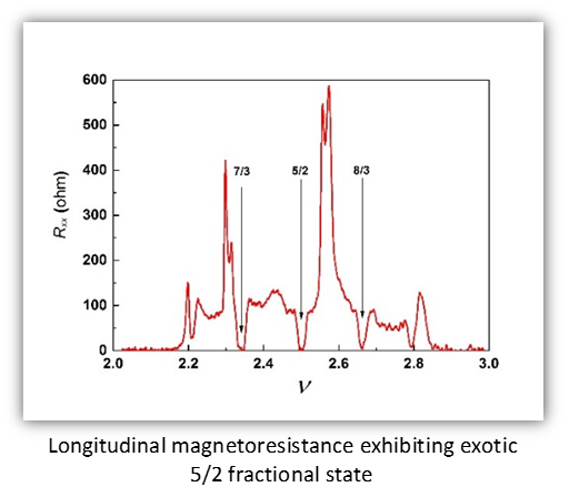 The Quantum Hall Effect (QHE), discovered in 1980 by Klaus von Klitzing, has still many open questions. Nowadays, many efforts are directed at the extremely fragile 5/2 fractional quantum Hall state, which is predicted to exhibit non-Abelian statistics, making it a candidate for fault-tolerant topological quantum computation. MBE growth of 2DEG structures that display a fully quantized 5/2 state provides a great challenge, requiring not only extreme material purity, but also distinctive design of the disorder potential landscape by utilizing special doping schemes.
Novel thermal transport measurements, recently developed in Prof. M. Heiblum group, allow access the state’s topological order, necessitating even more complicated structures - where thermal conductance via the doping layers and the bulk should be fully suppressed.
Exciton Liquid in Coupled Quantum Wells
 Excitons, bound states of electrons and holes, can be formed in semiconductors under photoexcitation, and have long been predicted to form correlated phases at sufficiently large densities and low temperatures. Studies of an exciton liquid as well as exciton gas-liquid phase transition in coupled quantum wells (QW) are carried out in Prof. Israel Bar-Joseph group using MBE grown AlGaAs/GaAs wafers as a favorite platform. This project implies significant challenges for the MBE growth. High sensitivity of exciton photoluminescence properties both to the material purity and to the interface smoothness in narrow QWs, separated by a thin barrier, necessitates a special design of the epitaxial growth and the sequence of layers in order to minimize the interface roughness. Moreover, the experiments require epitaxial growth of optically transparent gates made of n+-GaAs, which are isolated from the QWs by AlGaAs low leakage potential barriers.
Artificial Helical Edge structures
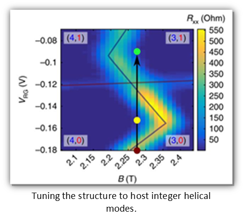 Electronic systems hosting one-dimensional helical modes with opposite spins have recently turned into an important field of research. Many materials, like InAs/GaSb/AlSb heterostructures, exhibiting strong spin-orbit coupling, have been suggested as the favored platform for these studies, but the anticipated spin protection from backscattering has not been confirmed. A new and alternative approach, enabling formation of robust and highly controllable helical modes in the QHE effect regime, utilizing high mobility AlGaAs/GaAs 2DEG, was developed in Prof. M. Heiblum group. This new technique is based on a ‘clever’ band-gap engineered MBE grown heterostructures, which contain a two-dimensional electron gas (2DEG), embedded in a so-called double quantum well (DQW), hosting two electronic sub-bands. By a proper electrostatic gating of two adjacent half-planes of the 2DEG, spin-split Landau levels, belonging to the different sub-bands, cross each other at the interface between the two half-planes, forming counter-propagating edge modes in the same lateral position.
Dislocation filters in AlGaSb/GaAs heterostructures
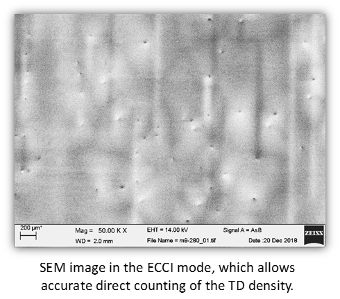 Lattice-mismatched heteroepitaxy is a growing field of research due to the possibility to expand significantly the range of useful semiconductor materials with important implications - both for basic and applied research. Among different lattice-mismatched systems Ga(Al)Sb/GaAs heterojunctions are of considerable interest both for III - Sb quantum devices, which have been predicted to exhibit topological insulator properties, and for a wide range of commercial electronic and optoelectronic devices, which may be grown on GaAs substrates. It was established that the lattice mismatch of about 8% in the GaSb-GaAs system might be almost fully compensated, at proper growth conditions, by so-called interfacial misfit array of 90° - type dislocations confined near the interface. However, the residual threading dislocations (TDs), propagating to the surface of the growing layers, often degrade material properties. We are developing the so-called ‘dislocation filters’ in the Ga(Al)Sb/GaAs material system using super-lattices comprising from layers with intentionally introduced elastic strains. Such an approach allows two orders of magnitude decrease in TDs density within 1.5÷2 micron thick buffer layer. The Electron Channeling Contrast Image method (ECCI), which utilizes backscattered electron detector, was adapted in our SEM in order to obtain a direct image of the TDs, and thus, to measure accurately their spatial distribution and density.