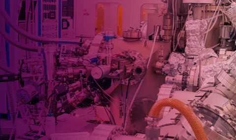
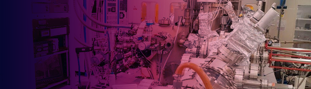
The Molecular Beam Epitaxy (MBE) laboratory, founded in 1991 in the Braun Center for Submicron Research, has a successful long track record in growing ultra-pure crystalline heterostructures from elements in the groups III & V of the periodic table. Since the year 2008 and on our MBE laboratory holds the world record electron mobility in ‘as grown’, ultra-pure AlGaAs/GaAs two-dimensional electron gas (2DEG). Two MBE systems are currently used to grow both high quality AlGaAs/GaAs heterostructures as well as InAs/GaSb/AlSb wafers with 2DEG embedded in InAs quantum well. These structures are used by numerous groups in the department of Condensed Matter Physics and worldwide for studies of Quantum Hall Effect, Majorana anyons, Topological Insulators, etc. The evolved MBE technology is a most advanced method for growing pure semiconductor crystals, and, may be, the only one that is able to grow ultra-pure semiconductor thin films with background impurities concentration well below 5×1013 cm -3. This technology allows building semiconductor structures with a resolution of one atomic layer, and thus, implement complex ‘band-gap engineering’ as well as to introduce, when required, controllable potential disorder in the 2D plane for advanced studies of correlated electron motion.
for high mobility semiconductors