


Halide Exchange in Single Crystal Halide Perovskites
Halide Perovskites (HaPs) with general the formula
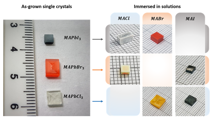
“Before/After” crystals. Left side of figure shows as- grown single crystals, right side shows post immersion crystals in the various solution. In the right matrix each row represents a different kind of
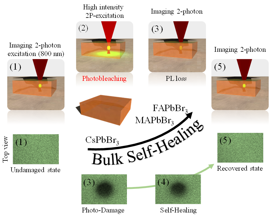
Self-Healing and Bulk Chemical Evolution of Photostimulated Reactions in Halide Perovskites
In this project we study the consequences of photo-stimulation of halide perovskites (HaPs) in the bulk. We investigate the chemical environment, kinetics and the influence that the environment can have on the bulk chemical properties of HaPs. Results of this project are of fundamental importance in defining the intrinsic stability and optical properties of HaPs.
On Ferroelectricity in Halide Perovskites
Halide peroskite (HaP) semiconductors are revolutionizing photovoltaic (PV) solar energy conversion by showing remarkable performance of solar cells made with esp. tetragonal methylammonium lead tri-iodide (MAPbI3). IN particular, the low voltage loss of these cells implies a remarkably low recombination rate of photogenerated carriers. It was suggested that low recombination can be due to spatial separation of electrons and holes, a possibility if MAPbI3 is a semiconducting ferroelectric, which, however, requires clear experimental evidence. As a first step we show that, in operando, MAPbI3 (unlike MAPbBr3) is pyroelectric, which implies it can be ferroelectric. The next step, proving it is (not) ferroelectric, is challenging, because of the material's relatively high electrical conductance (a consequence of an optical band gap suitable for PV conversion!) and low stability under high applied bias voltage. This excludes normal measurements of a ferroelectric hysteresis loop, to prove ferroelectricity's hallmakr switchable polarization. By adopting an approach suitable for electrically leaky materials as MAPbI3 , we show here ferroelectric hysteresis from well-characterized single crystals at low temperature (still within the tetragonal phase, that is stable at room temperature). By chemical etching we also can image teh structural fingerprint for ferroelectricity, polar domains, periodically stacked along the polar axis of the crystal, which, as predicted by theory, scale with the overall crystal size. We also succeeded in detecting clear second harmonic generation, direct evidence for the material's non-centrosymmetry. We note that the material's ferroelectric nature, can, but need not be important in a PV cell at room temperature.
- Rakita, Y., Meirzadeh, E., Bendikov, T., Kalchenko, V., Lubomirsky, I., Hodes, G., Ehre, D. and Cahen, D., 2016. CH3NH3PbBr3 is not pyroelectric, excluding ferroelectric-enhanced photovoltaic performance. APL Materials, 4(5), p.051101.
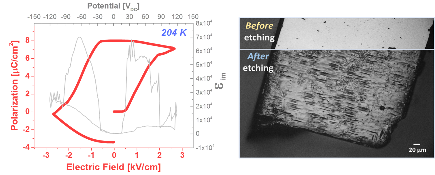
(Left) Ferroelectric response measurement: ΔP-E hysteresis loop obtained from integration of εim over EDC. The hysteresis loop is convoluted from a lossy bulk (i.e., resistor) response and ferroelectric polarization response. (Right) Evidence for ferroelectric polar domains: Bright field image from a light microscope of a crystal before and after etching in acetone for 120 sec.
Control Over Self-Doping in High Bandgap HaP's
While new information on high efficiency perovskite solar cells appears on a weekly basis, there are major gaps in our understanding of high bandgap perovskite devices; the selective contacts, doping, gap states and interface-related properties have not been thoroughly investigated in these materials. One of the questions is: what limits the open circuit voltages in high band gap (> 2eV) perovskite devices?
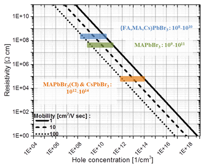
Estimated hole concentrations of the different HaPs, derived from dark resistivity measurements using equation (2), and the range of carrier mobility values, found in the literature. While MAPbBr3(Cl) and CsPbBr3 have an estimated hole concentration of 1012-1014 cm-3, in (FA,MA,Cs)PbBr3 and MAPbBr3 these are orders of magnitude lower, ~ 108-1010 cm-3.
To date, the highest reported VOC for perovskite solar cells is 1.65V using MAPbBr3 as the absorber, a perovskite semiconductor with a band gap of 2.3eV. Considering a thermodynamic limitation resulting in loss of ca. 0.3V between Eg and VOC, thre are gaps in our understanding as to 'where' and why do we lose the rest of the voltage. The aim is to study materials, as well as interface-related properties, to understand what limites the open circuit voltage in devices, based on high band gap (> 2eV) HaP's and related materials. Recently, we have shown that carefully selecting the combination of precursors in Br-based HaP absorbers allows some control over doping and charge transport properties in these materials. Four different bromide-based HaP's were used to show that, depending on the material composition, the optoelectronic properties can be dramatically changed. By introducing additional A cations to the precursor solution, the initial free hole concentration decreased by 1-4 orders of magnitude compared to the single cation equivalents, and two carriers charge transport properties were observed in the mixed A cation HaP, with electron and hole diffusion lengths of 640 and 990 nm, respectively. The multi A cation HaP-based solar cells are the first example of high band gap HaP-based solar cell devices with resemblance to p-i-n junction-like behavior.
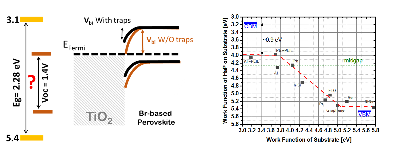
What Limits the Open-Circuit Voltage of Bromide Perovskite-Based Solar Cells?
High bandgap Pb bromide perovskite, APbBr3–based solar cells, where A is a mixture of formamidinium, methylammonium and Cs, show significantly higher, relative, VOC losses than their iodide analogs. Using photoluminescence-, external quantum efficiency- and surface photovoltage- spectroscopy measurements, we show the absence of any significant electronically-active tail states within the bulk of the (FA0.85MA0.1Cs0.05)PbBr3absorber. All methods confirm that EG = 2.28 eV for this Halide Perovskite, HaP. Contact potential difference measurements for this HaP, on different substrates, reveal a Z-shape dependence between the substrate work functions and that of the HaP, deposited on it, indicating that the HaP is relatively low doped, and that its Fermi level is affected by the substrate onto which it is deposited. We confirm results from electron beam-induced current (EBIC) and other measurements that most voltage loss of cells, made with these HaP films is at the HaP/selective-contact interface, specifically the TiO2/HaP one and provide a complete account of these cells’ VOC losses. Capacitance measurements indicate that 350 mV VOC could be gained by eliminating (fast) interfacial states, emphasizing the importance of interface passivation. Still, even passivating the TiO2/HaP interface cannot eliminate the band misalignment with Br-based HaPs.
Charge Carrier Dynamics and Recombination in HaP thin Films
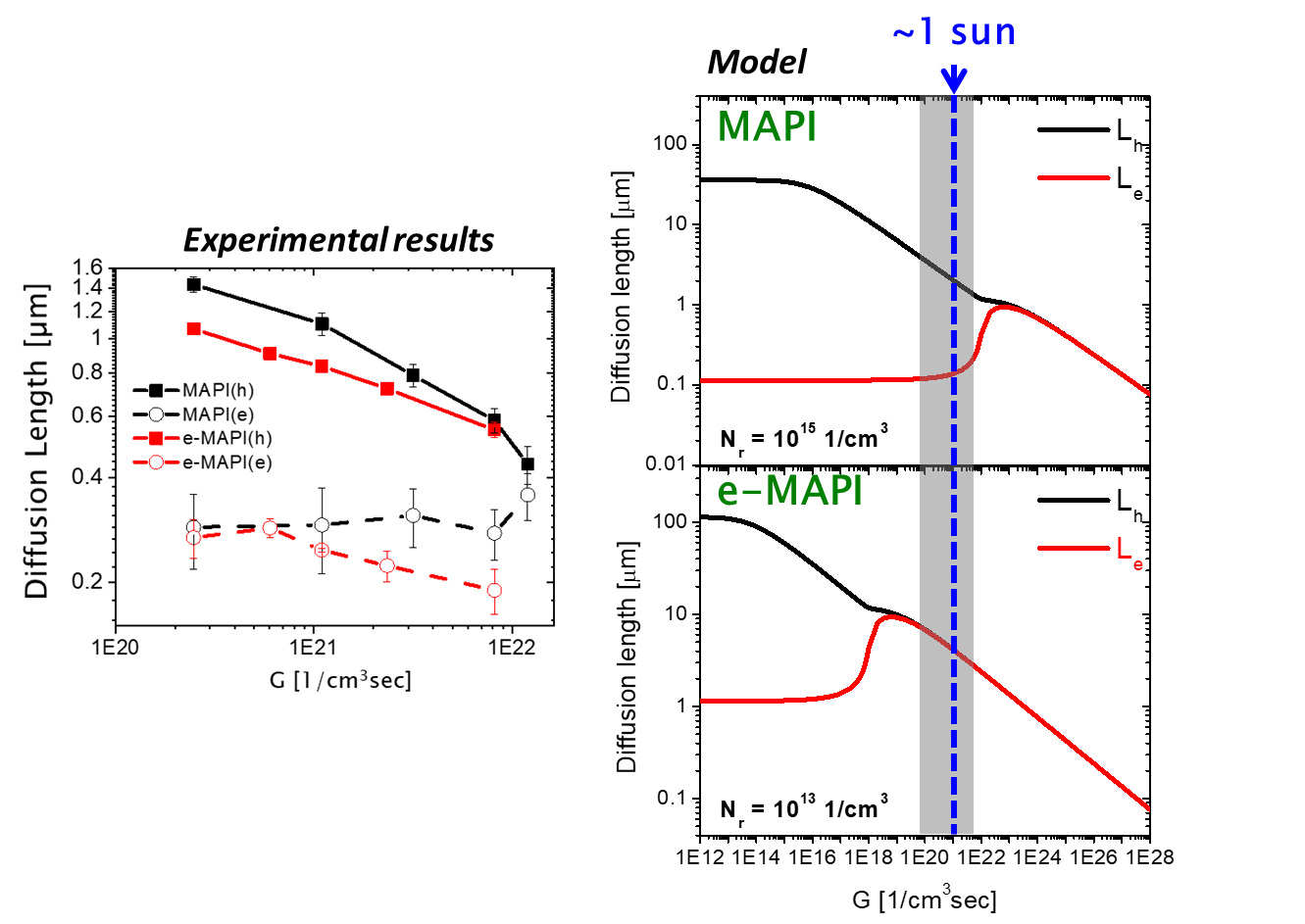
Photovoltaic solar cells operate under steady state conditions that are established during the charge carrier excitation and recombination. However, much of the research in the optoelectronic properties on these materials and cells relies on using illumination pulses of very short duration. Among these studies time-resolved photoluminescence (TRPL) has become one of the standard characterization tools of these systems. However, unlike the qualitative understanding and quantitative models that connect the cell parameters and quantities that are measured by steady state phototransport methods, the relation between these parameters and quantities derived by the transient parameters is not as clear. In particular, the steady state minority carrier diffusion length, is a critical quantity in the determination of the solar cell efficiency.
The basic question that arises, in particular in the context of the HaPs, is in how far the conclusions derived from the transient type of measurements (including photocurrent decay) are relevant to the steady state photoelectronic properties that determine the solar cell operation. In this research we focus on direct measurement of the electron and hole diffusion length (L) of HaPs, under steady state illumination conditions, as a function of the generation rate (G) and temperature, and show how a single type of recombination center model can explain our experimental results and resolve the dominant recombination mechanism as well as the trap density (Nr) in different types of MAPI films (solution processed and evaporated (e-MAPI)) in the given example shown in the Figure).
Levine, I., Gupta, S., Bera, A., Ceratti, D., Hodes, G., Cahen, D., Guo, D., Savenije, T.J., Avila, J., Bolink, H.J. and Millo, O., Can we use time-resolved measurements to get Steady-State Transport data for Halide perovskites? Journal of Applied Physics 124, 103103 (2018)
High bandgap perovskite devices
While new information on high efficiency perovskite solar cells appears on a weekly basis, there are major gaps in our understanding of high bandgap perovskite devices: the selective contacts, doping, gap states and interface-related properties have not been thoroughly investigated in these materials. One of the questions is: what limits the open circuit voltages in high band gap (> 2 eV) perovskite devices?
The lifetime of the CsPbI3-based cell is shown to be longer in every respect
Pb-free Inorganic Halide Perovskites as Opto-Electronic Materials
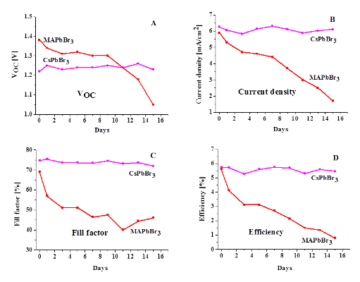
Over the past years there is tremendous growing interest in Hybrid Organic Inorganic metal halide Perovskite—HOIP (primarily methyl ammonium lead trihalides CH3NH3PbX3)-based solar cells. These cells demonstrated power conversion efficiencies of over 20% for very small cells, up from a few % within a brief period of research (~5 years). Recently, we showed that use of the all-inorganic halide perovskite CsPbBr3 can yield as good a PV performance, and a more stable one than the organic-inorganic hybrid one MAPbBr3.
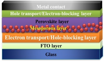
Schematic of a perovskite photovoltaic cell
with a mesoporous hole blocking layer
The role of the electrical contacts in organic- and metal-organic-based optoelectronic devices.
In this research we investigate the role of the electrical contacts on the electronic properties of the hybrid organic-inorganic perovskite (HOIP) via two strategies:
(1) using a solar cell device structure, in which the HOIP absorber layer is sandwiched between different n- and p-type contact layers as selective contacts, and
(2) in a simple Metal-Semiconductor configuration using different metals (or TiO2) as substrates.
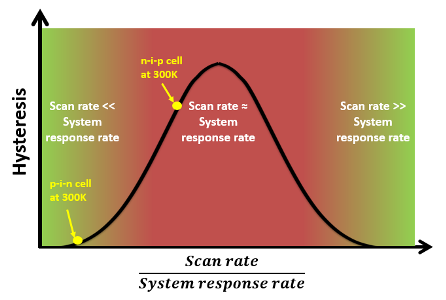
Explanation of hysteresis observed in pin and nip cells
Understanding the unique formation chemistry of halide perovskites
The achievement of high-quality optoelectronic properties in halide perovskite semiconductors through low-temperature, low energy processing is unprecedented. Understanding the formation process of these semiconductors is a critical step toward understanding the origins of high-quality via these simple preparation procedures.
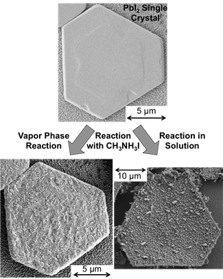
SEM image of a single PbI2 crystal before and after
reaction with MAI in solution and vapor phase
The effect of composition on the thermodynamics of charge carrier mobilities in perovskites
In those hybrid organic-inorganic perovskites which were previously used to form efficient solar cells, the A cation is organic; however, recent work from our group utilized the perovskite CsPbBr3 to produce a solar cell with an efficiency which is comparable to the efficiencies our lab has achieved for MAPbBr3-based devices. Despite the efficiency of the CsPbBr3 cell, as of September 2015 no one has yet attempted to quantify, with a direct comparison, how the replacement of the organic cation with cesium affects the transport properties of the perovskite material itself. Considering that the organic MA and FA ions have dipoles, whereas Cs does not, some have surmised that this dipole gives rise to ferroelectricity or other effects which may be responsible for the characteristically long carrier lifetimes observed in perovskites. Therefore, an improved understanding of the differences in transport properties between the hybrid organic-inorganic perovskites and the all-inorganic cesium perovskites could enhance our knowledge of those physical processes responsible for the high efficiencies of perovskite solar cells. We seek to understand how the substitution of an organic cation such as MA with an inorganic one such as Cs affects the electronic transport properties of the material. More specifically, another group has recently published measurements of mobility in MAPbI3 by terahertz spectroscopy which strongly suggest that the mobilities of the charge carriers are limited only by vibrations in the material. We seek to verify whether this finding holds on a larger scale for both MA and Cs lead halide perovskites. To that end, we conduct current-voltage and capacitance-voltage measurements at various temperatures across the materials’ phase transitions. The observation of a similar dependence of mobility upon temperature for all of the lead halide perovskites, together with previous work from our group showing similar mechanical properties for all members of the family, would demonstrate a general principle that the mobilities of lead halide perovskites are determined only by mechanical vibrations.
Interface Modifications of Semiconductors to Control Charge Transport in Photovoltaics
Halide perovskite (HaP)-based photovoltaic (PV) devices have reached ~20% power conversion efficiency within a few years of research. However, HaP-based PV cells still suffer from limited reproducibility, stability and incomplete understanding of how they work. Understanding the electronic processes involved in the PV charge transport, esp. those concerning the HaP interfaces in the cells, should allow to improve cell preparation and enhance device performance.
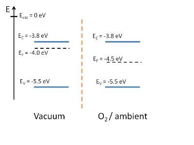
Fermi level position of MAPbI3 film on HOPG after exposure
to vacuum (left) and O2 (right). The n-type doping of the film
in vacuum decreases after O2/air exposure.
Understanding the Bulk Properties of Halide Perovskites for Photovoltaic Applications
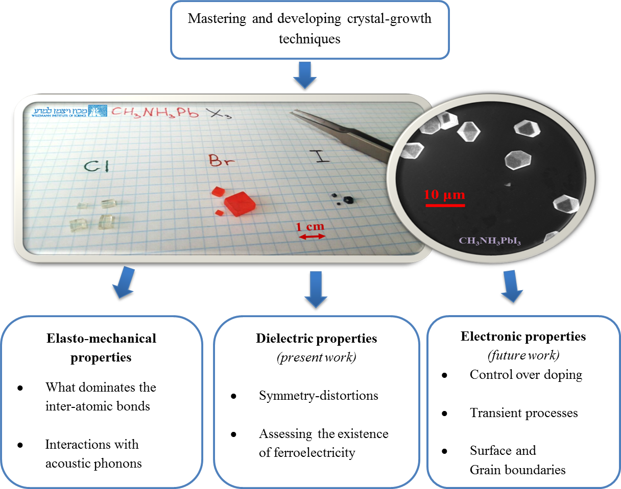
The ability to grow perovskite single crystals opens up many new avenues of research.
To understand what stands behind the success of halide perovskites, we address our research towards the main core of this new technology – the material. Since we are dealing with a complex system of an integrated organic and inorganic framework, we want to understand whether it possesses unique properties, how these influence photovoltaic performance and, more importantly, whether we can direct the field toward new materials with desired properties.
To achieve that, we start with growing single-crystals of the halide perovskites in their pure form – having the ability to grow them from several microns up to centimeters. Having that, we wish to answer questions that their answers should lead us towards a better understanding of the fundamental properties of these materials, to improve their integration in future devices and draw guidelines towards the next generation of materials for photovoltaics.