
MIMO Reduced RF Chain Demo
Executive Summary
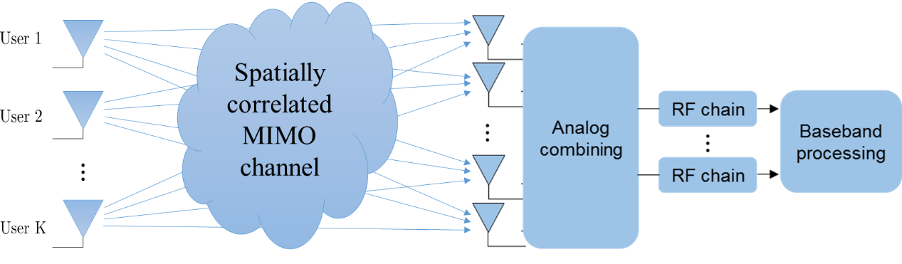
Massive multiple-input multiple-output (MIMO) communication is a key technology for future wireless systems as its increased spectral efficiency compared to conventional MIMO architectures. Theoretical benefits of utilizing the large-scale antenna arrays are well-established, while implementing massive MIMO in practice is a challenging task. One of the challenges encountered in such systems is the dramatic increase in hardware complexity. Due to the massive number of antennas and the relatively high cost and power consumption of RF chains, allocating a dedicated RF chain per each antenna as in conventional MIMO scheme is infeasible. It is therefore desirable to reduce the number of RF chains. In this demonstration, we address the hardware complexity challenge in a single-cell multi-user MIMO system, focusing on the task of estimating the underlying channel. In order to reduce the number of receive RF chains, we present a hardware prototype implementing analog combining for RF chain reduction. The prototype consists of a specially designed configurable combining board as well as a dedicated experimental setup. We adopt the Kronecker channel model with known second-order statistics of the channel (i.e., transmit and receive side covariance matrices), and show that the optimal combiner corresponds to the first eigenvectors of the receive side covariance matrix. Afterwards, the channel estimation with reduced receive RF chains is realized following a Bayesian approach, by applying the minimum mean squared error (MMSE) channel estimator to the output of our proposed analog combiner. The experimental study, which focuses on channel estimation accuracy in MIMO channels, demonstrates that using the proposed prototype, the achievable channel estimation performance is within a small gap in a statistical sense from that obtained using a costly receiver in which each antenna is connected to a dedicated RF chain. This prototype is developed at the Weizmann Institute of Science and was demonstrated at International Conference on Acoustics, Speech and Signal Processing (ICASSP) at Brighton, UK in May 2019.
Experimental Environment
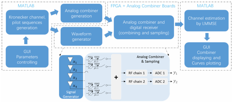
Our hardware prototype implements a configurable analog combiner, which is evaluated using a dedicated experimental setup at microwave frequencies. This setup consists of a Matlab-based host application and a FPGA board. The former simulates the Baseband (BB) channel output and processes the signal captured after analog combining. The latter acts as an interface between the digital signals generated and processed by the host application, and the analog signals which are utilized by the analog combiner hardware. In particular, the input and output signals of the analog combiner hardware are generated as follows:
- Analog combiner input: The digital baseband channel outputs simulated by the host application are transferred by an Ethernet cable from the host application to the FPGA board in real-time. The FPGA board generates the baseband input signal which is up-converted on the combiner board using a carrier waveform generated by a VSG25A vector signal generator. The resulting analog passband signal represents the multivariate channel output observed at the BS antenna array.
- Analog combiner output: The analog combined passband signal, representing the signal fed to the RF chains at the BS, is down-converted with the same carrier waveform as for the up-conversion on the combiner board, followed by an analog-to-digital conversion implemented on the FPGA. These digital outputs are transferred from the FPGA board to the host application where they are utilized for estimating the underlying channel. The host application is also capable of adjusting the weights of the analog combining hardware via the FPGA board. The experimental procedure is illustrated in the flow chart in Fig. 2.
Analog Combiner Implementation:
The most common is arguably a controllable network of fully connected phase shifters, i.e., the Phase-Shifter-Only Analog Combiner (PSOAC). Alternative architectures include fully connected complex gain networks, such as the Complex-Gain Analog Combiner (CGAC); fully connected phase shifters and switches network, and flexible partially connected phase shifters network with sub arrays. In order to incorporate a large family of architectures, our analog combiner hardware consists of a controllable network of gains and phase shifters. The outputs of the adjustable gains and phase shifters are then summed by a combiner and fed to an RF chain. In particular, our hardware system consists of 4 input ports and 2 output ports, namely, it can be utilized in a BS with 4 antennas and 2 RF chains. This setup can also be used for experimenting with analog combiners with larger number of antennas and RF chains using a virtual channel extension. By using the flexible and controllable network of gains and phase shifters, we implement the proposed designs for both CGACs as well as PSOACs. The baseline is to use the hardware board which models a MIMO BS with 4 antenna inputs and 2 RF chains. While this combiner implements a hybrid MIMO receiver with N_bs=4 and N_rf=2, it can also be used, along with the experimental setup detailed in the sequel, to evaluate in hardware hybrid MIMO BS with 8 antenna inputs and 4 RF chains as well as 16 antenna inputs and 8 RF chains. The ability to use the board and the experimental setup to evaluate hybrid receivers with larger number of antennas and RF chains is obtained using a virtual channel extension. This virtual channel approach is based on a sequential utilization of the basic hardware to obtain an overall combined result. For the realization of 8 antenna inputs and 4 RF chains, we need to sequentially utilize the basic hardware four times to complete the divided 4 blocks of the analog combiner matrix. A setup with 16 antenna inputs and 8 RF chains can be obtained by utilizing 16 different 4×2 basic combiners to complete the divided 16 blocks of the analog combiner matrix. Clearly, analog combiners with different analog combining ratios, namely, in which the number of antennas is not twice the number of RF chains, can be realized following the same guidelines by using only the required number of input and output ports.
System Description
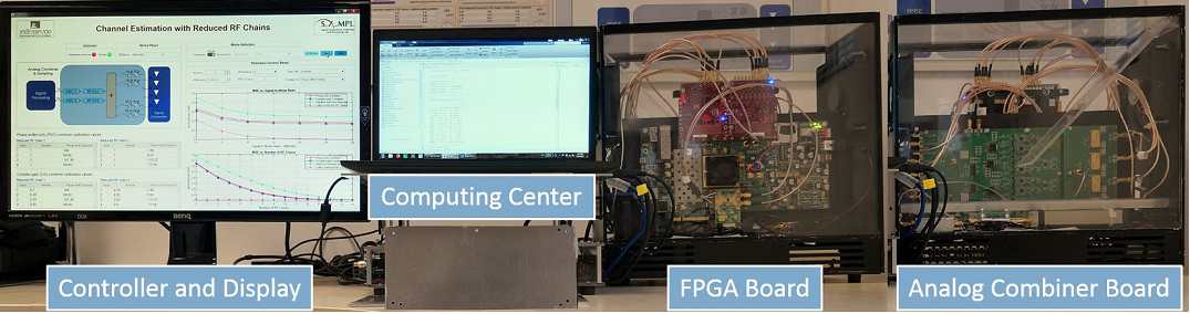
The overall prototype system is depicted in Fig. 3. The prototype consists of the following components: a controller and display, providing the GUI, a computing center running the Matlab-based host application, an FPGA board, and the analog combiner hardware.
Controller and Display
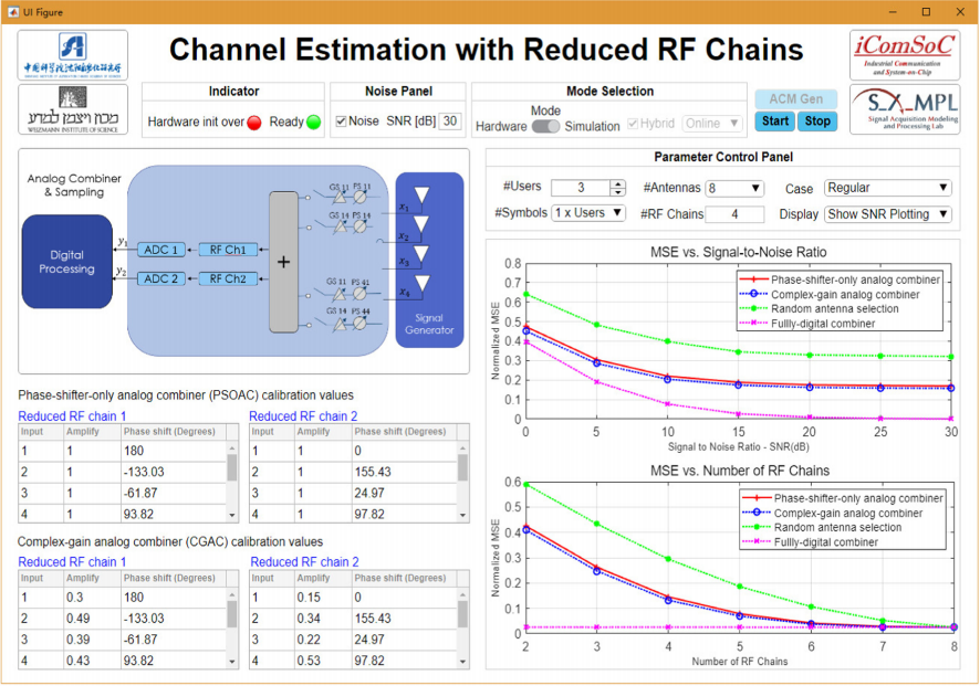
The GUI allows to configure and evaluate the experimental setup in a user-friendly environment. In particular, our GUI provides the ability to change the main parameters of the experiment and to numerically compare the normalized MSE obtained in two display modes: with respect to SNR or number of RF chains. The main controllable parameters include the number of UT, training symbols, receive antennas, and the rank of the receive side correlation matrix. Details of the supported parameter combinations are summarized in Table 1.

Once the experimental setup is configured and a test is launched, the GUI presents in real-time the selected values used to configure the analog combining hardware for both PSOAC as well as CGAC. Furthermore, the GUI presents updated normalized MSE curves during the test and after it is concluded, comparing the performance of the utilized PSOAC and CGAC to analog combiners in which the RF chains are directly connected to randomly selected antennas, as well as to a fully-digital setup. The fully-digital setup, representing the performance achievable without analog combining when each antenna feeds a dedicated RF chain, constitutes a fundamental lower bound on the channel estimation MSE with RF chain reduction. An overview of the GUI is depicted in Fig. 4.
Computing Center
The computing center is a 64-bit laptop with 4 CPU cores and 16GB RAM running the Matlab-based host application. The application is controlled by the GUI, and implements the following functionalities:
- The host application computes the analog combiner weights, and adjusts the analog combiner hardware before each simulation test.
- The application generates the digital baseband signals, i.e., the pilot sequences, as well as the wireless channel outputs, which are fed to the FPGA to generate the analog combiner input.
- On the receive side, the application processes the baseband channel outputs and produces the MMSE channel estimate.
The communication between the computing center and the hardware board is carried out over an Ethernet cable. Through the cable, the generated digital baseband channel outputs and analog combiner matrix are transmitted to the build-in memory of the FPGA board, and the baseband RF chain outputs are acquired.
FPGA Board
The FPGA board consists of an off-the-shelf Xilinx VC707 evaluation board. The evaluation board utilizes a 4DSP FMC204 16-bit DAC mezzanine card for baseband waveform generation, as well as an eight-channel 4DSP FMC168 16-bit digitizer card for sampling of the combined analog signal.
In the baseband analog signal generation process, the waveforms are stored as digital baseband I/Q pairs on the build-in memory. Then, the FPGA device reads out the pre-stored waveforms from the memory and employs an 8Gbps Serializer/Deserializer (SerDes) device to transfer it to the 16-bit DAC mezzanine card. The DAC card then interpolates and converts the stored waveforms to analog baseband signals at a sample rate of 250Msps. The analog baseband signals are transmitted to the analog combiner board through coaxial cables where they are up-converted to passband and linearly combined.
The analog combiner outputs, which are down-converted to baseband on the combiner board, are digitized using four out of eight channels of the 16-bit digitizer card with a 250MHz sampling rate. Each I/Q pair occupies two channels of the digitizer card. The 1.2Gbps SerDes transfers the sampled data to the FPGA who then writes the data to a digital first-in-first-out (FIFO) buffer for reading by the computing center.
The FPGA also produces selection and control commands for configuring of analog combiner. Once the host application produces an analog combiner configuration, the weights matrix is provided to the FPGA board via the FIFO buffer. These weights are then transferred to the analog combiner hardware using a serial peripheral interface (SPI) protocol, which is used to control the dedicated analog combiner board.
Analog Combiner Board:
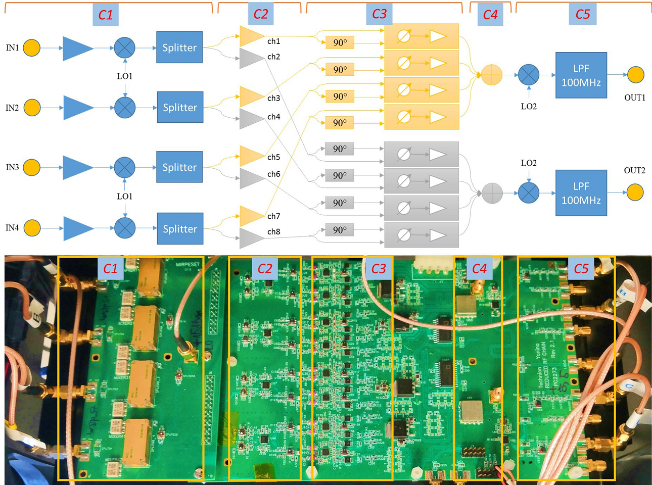
The analog combiner board is a self-designed dedicated hardware, which realizes a controllable analog combiner network, and can serve as any of the common combiner architectures, e.g., phase shifter networks, switching networks and DFT beamforming. The designed analog combiner supports two different types of input signals: one is passband signals in the frequency band up to 4.5GHz and another is BB signals each with a 125MHz maximum bandwidth. In our experimental setup we use BB signals as our inputs, where up-conversion and down-conversion are carried out on the analog combiner board. The board consists of five different blocks, implementing the main different functionalities, namely:
- Up-conversion of incoming signal and signal splitting.
- Passband signal input and amplification.
- Weights (phases and gains) application and configuration.
- Summing up of the incoming signals.
- Down-conversion and low-pass filtering of combined signals.
The individual blocks of the analog combiner board are marked in Fig. 5, which depicts the block diagram of the hardware as well as the circuit board.
In block C1, each of the four inputs is a complex BB signal transmitted from the FPGA, feeding an amplifier followed by a mixer. The BB signals whose maximal range of frequency is 125MHz are up-converted to RF signals at a frequency of 1GHz. The RF signals represent the passband signals observed by the BS antennas and each power level of the RF signals are tuned to 0dBm and split into two same signals. In order to support passband inputs, one must only replace block C1 with the corresponding passband signals observed by the antennas.
Each of the passband signals is forwarded to block C2, where it is fed to an amplifier with 16dB fixed gain. Specifically, we use an ADL5566 dual RF operational amplifier for each splitted pair of passband signals. This amplifier has a low latency and a very flat frequency response, including a channel-to-channel gain and phase errors of 0.1dB and 0.06o, respectively, at 100MHz. Furthermore, the ADL5566 supports input signals with up to 4.5GHz bandwidth without having the amplification vary over frequency, while hardly affecting the SNR due to its low noise input stage of only 1.3nV/√Hz. Thus, the receiver contains four ADL5566 amplifiers for the four RF input signals. The wideband range property of ADL5566 makes our hardware suitable for a broad range of RF signals used in actual communication systems.
The signals from the amplifiers are separated into two groups. Each group has four inputs, including one signal from each splitted pair. Then, each signal is splitter again into two signals with 90o offset, which are used as the inputs to a phase shifter and gain block. The purpose of this additional splitting with phase offset stems from the fact that we use differential phase shifters which operate on such inputs. In block C3, each of the four channels in one of the groups is activated by an ADL5390 analog vector multiplier, implementing the phase and gain of each analog combining weight applied to the input signal. The weights applied in the vector multiplications are determined by the output DC level of an AD7808 octal 10-bit DACs with serial load capabilities, which receives control commands from the FPGA board used to configure the analog combining weights by finding a look-up table. The usage of controllable gains and phases requires a calibration stage when the interconnections are established to guarantee that the configured weights are correctly translated into the desired phase and gain values.
The outputs of each group are summed in block C4, which finalizes the realization process of analog combining and obtains a combined passband signal. Then, the combined signals are down-converted in block C5 using a set of ADL5382 down-converters with the same local oscillator used for up-conversion. The down-converted signals are filtered to baseband signals with a maximum 125MHz bandwidth. Finally, the signals of the two outputs are forwarded to the FPGA where they are acquired using a 4DSP FMC168 16-bit digitizer card, obtaining the digital outputs for further digital signal processing in the computing center.
Experimental Results
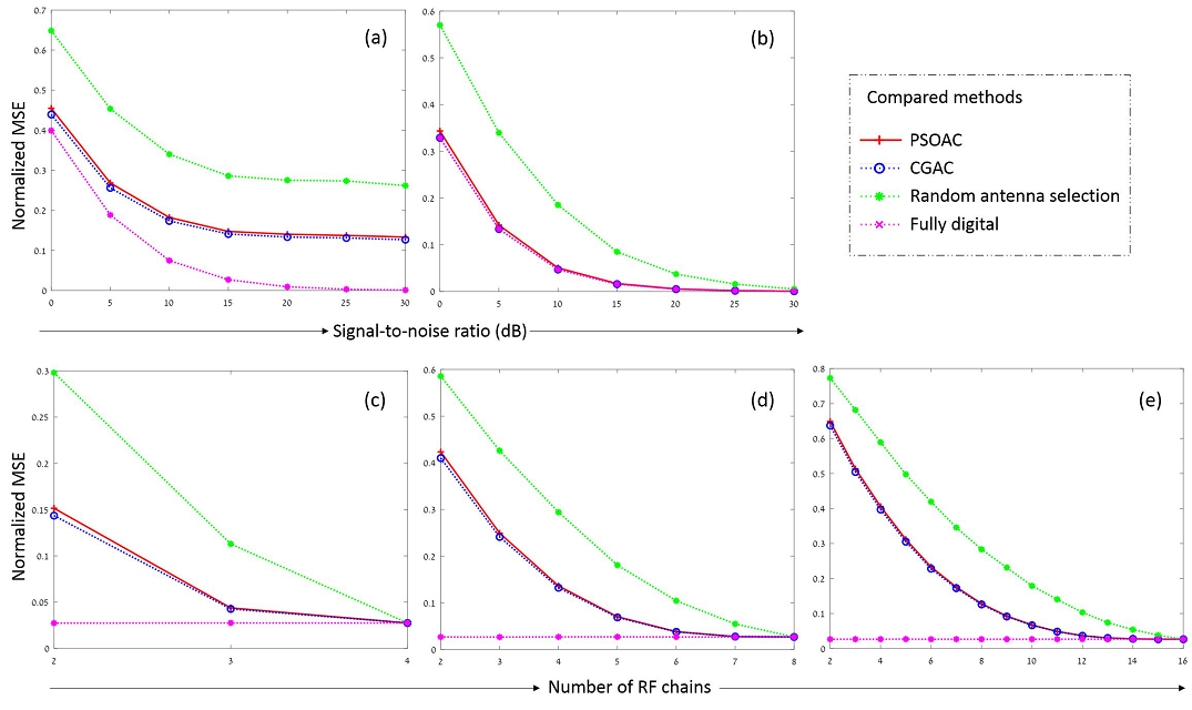
In the experimental study, we evaluate the channel estimation performance when the observed channel output is combined using our analog combining hardware, configured as both a CGAC as well as a PSOAC. While we focus here on MSE channel estimation, the proposed analog combiner can be used to evaluate various other measures, such as bit error rate, by using different processing of the combiner output, e.g., symbol detection, in the digital domain. The channel estimation accuracy is compared to that achievable when using a random antenna selection, which randomly selects N_rf out of N_bs antennas, and also to the traditional fully-digital setup, where each antenna is connected to a dedicated RF chain.
Normalized MSE versus SNR
We first test the normalized MSE in estimating the channel versus SNR in the range [0,30]dB, for an analog combiner with N_bs=8 antennas and N_rf=4 RF chains. Note that this analog combiner model is obtained using the virtual channel extension approach. The results are depicted in Figs. 6(a)-6(b) for high rank (regular) receive correlation and for low rank (best) receive correlation, respectively. Observing Figs. 6(a)-6(b), we note that using the proposed hardware prototype, the PSOAC achieves channel estimation accuracy within a very small gap compared to the costly CGAC architecture. Furthermore, both PSOAC and CGAC architectures notably outperform the random antenna selection approach. It is noted however that random antenna selection is simpler to implement compared to analog-combiner based systems, which require additional hardware. As expected, the fully-digital architecture achieves the lowest MSE performance, as it has access to the observed channel output without dimensionality reduction.
For the high rank (regular) receiver correlation case, it is seen in Fig. 6(b) that all approaches which implement analog combining meet an error floor at high SNR (above 20dB). This error floor is due to the model mismatch induced by the dimensionality reduction, which becomes the main performance bottleneck at this SNR regime. However, when the rank of the receive correlation matrix is not larger than the number of RF chains, the optimal MSE performance observed using fully-digital receivers is also achievable using our analog combiner prototype.
Normalized MSE versus Number of RF Chain
Next, we numerically evaluate the normalized MSE performance achievable using our hardware analog combiner prototype for different numbers of RF chains. Here, we let the number of RF chains N_rf vary in the range of [2,N_bs ], for a fixed SNR level of 15dB, and for a high rank (regular) receive correlation setup. The results of this experiment are depicted in Figs. 6(c), 6(d) and 6(e), for N_bs={4,8,16}, respectively. Observing Figs. 6(c)-6(e), we note that for all considered scenarios the normalized MSEs of our hybrid architectures approach the normalized MSEs of the fully-digital receiver as the number of RF chains increases. This result settles with the fact that for N_rf=N_bs these networks implement a fully-digital receiver. When the reduction rate N_rf⁄N_bs is above 62.5%, the performance gaps between the proposed analog combiners and the fully-digital receiver become negligible. This behavior is due to the numerical observation that most simulated channels can be reliably characterized by roughly 5⁄8 of their eigenmodes, which are reliably recovered and restored using our analog combiner hardware prototype. Moreover, among the hybrid receivers, the PSOAC achieves normalized MSE values which are only slightly higher than that of the costly CGAC. Finally, both the CGAC as well as the PSOAC have lower normalized MSEs than the random antenna selection.
These results demonstrate the ability of our proposed configurable analog combiner hardware to efficiently implement desirable RF chain reduction while inducing minimal performance degradation on the overall communication system.
References
- T. Gong, N. Shlezinger, S. S. Ioushua, M. Namer, Z. Yang, and Y. C. Eldar, “RF chain reduction for MIMO systems: A hardware prototype", IEEE Systems Journal, vol. 14, no. 4, pp. 5296-5307, December,2020.
- S. S. Ioushua and Y. C. Eldar, “A family of Hybrid Analog-Digital Beamforming Methods for Massive MIMO systems", IEEE Transactions on Signal Processing, vol. 67, no. 12, pp. 3243–3257, June 2019.