

Energy dissipation is a fundamental process governing the dynamics of physical, chemical and biological systems. It is also one of the main characteristics that distinguish quantum from classical phenomena. In particular, in condensed matter physics, scattering mechanisms, loss of quantum information or breakdown of topological protection are deeply rooted in the intricate details of how and where the dissipation occurs. Yet the microscopic behavior of a system is usually not formulated in terms of dissipation because energy dissipation is not a readily measurable quantity on the micrometer scale. Although nanoscale thermometry has gained much recent interest, even the best existing thermal imaging methods are not sensitive enough for the study of quantum systems and are also unsuitable for the low-temperature operation that is required.
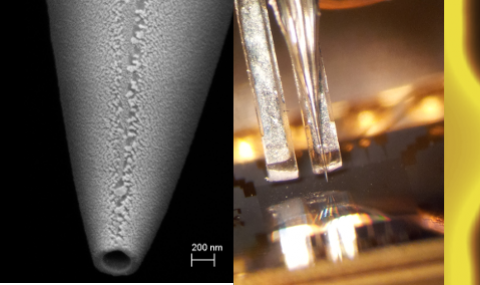
SQUIDs are commonly known to be very sensitive sensors of magnetic flux. The source for their sensitivity is the strong dependence of the critical current on magnetic field. The critical current, however, is also temperature dependent. In our lab we used this concept to develop a novel nano-thermometer based on a superconducting quantum interference device (tSOT: SQUID-on-tip thermometer) with a diameter of less than 50 nm that resides at the apex of a sharp pipette. This tool provides scanning cryogenic thermal sensing that is 104 times more sensitive than previous room-temperature thermal imaging devices, allowing the detection of a sub 1 μK temperature variations. Furthermore, it is non-contact and non-invasive and allows thermal imaging of very low intensity, nanoscale energy dissipation down to the fundamental Landauer limit of 40 fW for continuous readout of a single qubit at 1 GHz at 4.2 K.
Since the device is SQUID based it can be tuned to be sensitive to magnetic signals as well. Figure 1 demonstrates a simultaneous measurement of thermal and magnetic signals in a composite nanowire.
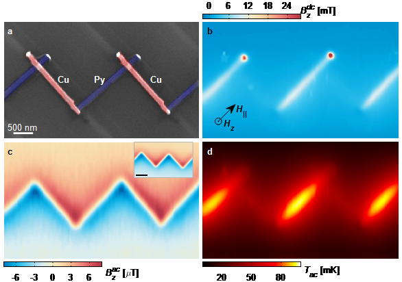
Image 1 | Simultaneous scanning tSOT thermal and magnetic imaging. a, False color SEM image of zigzag structure of alternating Cu (red) and Py (blue) nanowires. b, Image of Bzdc in presence of applied magnetic field revealing the in-plane magnetization of Py segments. c, Bzac due to applied ac current of 10 µA through the structure. Inset: Theoretically calculated signal. d, Thermal image showing enhanced dissipation in the Py segments due to their significantly higher resistivity. All signals were acquired simultaneously.
We use this exciting tool for direct investigation of dissipation processes in operating microscopic electronic devices and novel states of matter. We were able to observe changes in dissipation due to single-electron charging of individual quantum dots in carbon nanotubes (see Fig. 2).
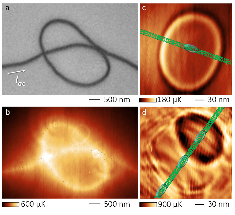
Fig. 2 | Thermal imaging of single-walled carbon nanotubes and scanning gate thermometry of quantum dots. (a) SEM image of looped single-walled CNT carrying Iac= 12 nA. (b) Thermal image acquired by tSOT at 4.2 K. Dotted line shows the outline of the CNT. The fine ring-like structures result from quantum dots along the CNT. (c) Zoomed-in thermal image of a thermal ring of a single QD resulting from Coulomb blockade due to single electron charging. Overlaid is a cartoon of CNT with a QD. (d) Similar thermo-spectroscopy measurement showing concentric thermal rings around three schematically shown QDs.
One of our exciting results is the discovery of dissipation due to resonant localized states in high mobility graphene devices. This observation provides insight into the fundamental question of how electrons thermalize in a clean system. In pristine graphene structures, the mean-free path of electrons is typically larger than the size of the device and the electron–phonon coupling is very weak. As a result, ‘hot’ electrons injected into the device are scattered elastically multiple times and are trapped within the device without being able to dispose of their excess energy. Our thermal imaging revealed remarkable heat patterns, showing that the materials defects naturally formed at the edges of graphene structure act as atomic-scale ‘beacons’ that provide highly-localized resonant electron–phonon coupling pathways for disposing the excess energy of hot electrons (see Figs. 3 and 4).
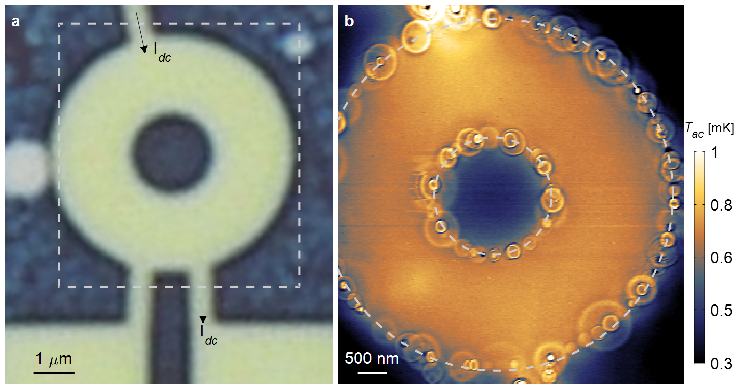
Fig. 3 | Novel dissipation mechanism in hBN encapsulated graphene sample. Scanning gate tSOT thermometry image reveals a heat transfer process which is mediated by edge defects.
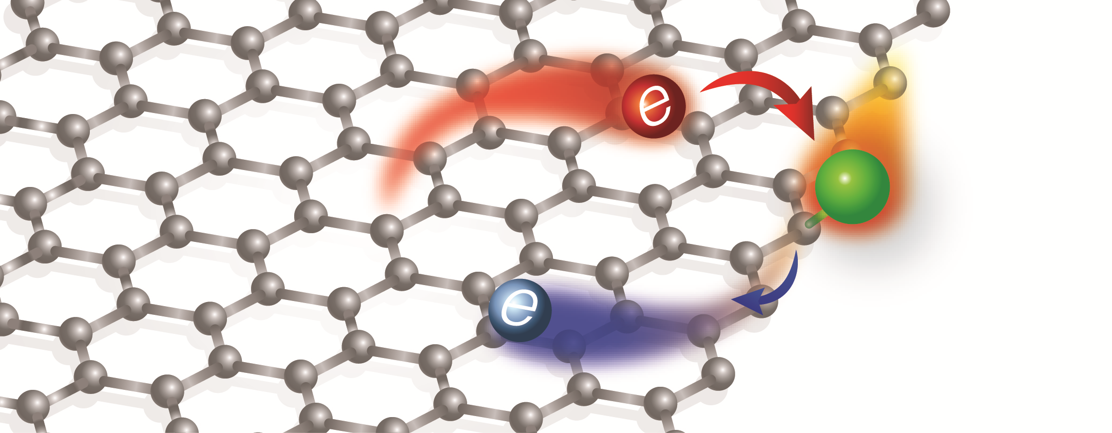
Fig. 4 | A schematic illustration of hot electron relaxation in pristine graphene. A hot electron (red) inelastically scattered by a localized state at the edge of graphene and is reflected at a lower energy (blue). As a result heat is dissipated in the defect.
The tSOT thermometry technique and measurements are described in:
D. Halbertal, J. Cuppens, M. Ben Shalom, L. Embon, N. Shadmi, Y. Anahory, H. R. Naren, J. Sarkar, A. Uri, Y. Ronen, Y. Myasoedov, L. S. Levitov, E. Joselevich, A. K. Geim, and E. Zeldov, Nature 539, 407–410 (2016), http://dx.doi.org/10.1038/nature19843, full text (view only).
The work was awarded the 'Outstanding Paper Award' for 2016 by the European Microscopy Society (EMS)
Commentary by Prof. Bertrand Halperin (Harvard) in Journal Club for Condensed Matter Physics:
http://www.condmatjournalclub.org/?p=2908
Imaging resonant dissipation from individual atomic defects in graphene:
Dorri Halbertal, Moshe Ben Shalom , Aviram Uri, Kousik Bagani , Alexander Y. Meltzer , Ido Marcus, Yuri Myasoedov ,John Birkbeck , Leonid S. Levitov ,Andre K. Geim, Eli Zeldov http://science.sciencemag.org/content/358/6368/1303
Commentary by Prof. Anton Akhmerov (Delft) in the Journal Club for Condensed Matter Physics:
https://www.condmatjclub.org/uploads/2018/05/JCCM_May_2018_01.pdf
News Article in IOP NanotechWeb:
http://nanotechweb.org/cws/article/tech/66769
News Article in IsraelBDS:
http://israelbds.org/looking-for-hot-spots-in-cold-places/