
SQUIDs
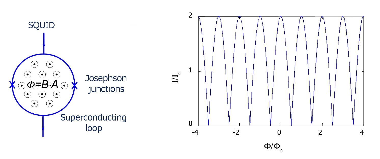
A SQUID is schematically described by a superconducting loop with two weak links. The maximal current that can flow in the SQUID without dissipation is periodic in flux in the loop
Ic(Φ) = I0|cos(π Φ/Φ0)|.
nanoSQUID on a tip
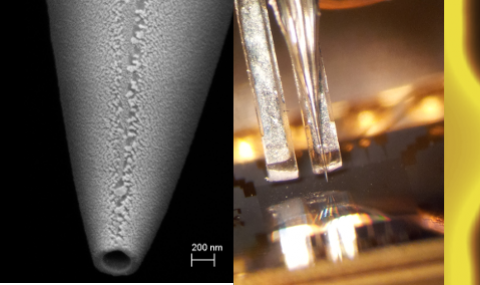
In recent years there is a growing interest in development of microSQUIDs and nanoSQUIDs for imaging and study of quantum magnetism. Imaging magnetic fields on a nanoscale is a major challenge in nanotechnology, physics, chemistry, and biology. One of the milestones in this endeavor is to achieve sensitivity sufficient for detection of the magnetic moment of a single electron. There are three main technological challenges: fabrication of a sensor with a high magnetic flux sensitivity, reducing the size of the sensor, and the ability to scan the sensor nanometers above the sample. Most of the current microSQUIDs are based on planar technology using lithographic or focused ion beam patterning methods. The planar geometry, however, prevents bringing the SQUID loop into sufficiently close proximity to the sample (due to alignment issues). We have developed a self-aligned fabrication method of smallest SQUIDs in the world which does not require any lithographic or processing steps. In addition, the major advantage is that this nanoSQUID resides on the apex of a very sharp tip that is ideally suited for scanning probe microscopy. The resulting SQUID-on-tip (SOT) made of Pb has an effective diameter of below 50 nm and flux noise of down to Φn = 50 nΦ0/Hz1/2 at 4.2 K that is operational up to unprecedented high fields of 1 T. The corresponding spin sensitivity of the device is Sn = 0.38 μB/Hz1/2, which is about two orders of magnitude more sensitive than any other scanning SQUID to date.
SQUID on tip fabrication
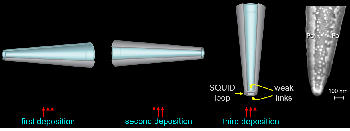
nanoSQUID on tip fabrication recipe.
Additional information
- A scanning superconducting quantum interference device with single electron spin sensitivity
D. Vasyukov, Y. Anahory, L. Embon, D. Halbertal, J. Cuppens, L. Neeman, A. Finkler, Y. Segev, Y. Myasoedov, M. L. Rappaport, M. E. Huber and E. Zeldov
Nat. Nano 8, 639 (2013) - Scanning superconducting quantum interference device on a tip for magnetic imaging of nanoscale phenomena
A. Finkler, D. Vasyukov, Y. Segev, L. Ne'eman, E. O. Lachman, M. L. Rappaport, Y. Myasoedov, E. Zeldov, and M. E. Huber
Rev. Sci. Instrum. 83, 073702 (2012). - Self-aligned nanoscale SQUID on a tip
A. Finkler, Y. Segev, Y. Myasoedov, M. L. Rappaport, L. Ne'eman, D. Vasyukov, E. Zeldov, M. E. Huber, J. Martin and A. Yacoby
Nano Letters 10, 1046 (2010) - Electrically tunable multi-terminal SQUID-on-tip
Aviram Uri, Alexander Y. Meltzer, Yonathan Anahory, Lior Embon, Ella O. Lachman, Dorri Halbertal, Naren HR, Yuri Myasoedov, Martin E. Huber, Andrea Young, Eli Zeldov
arXiv:1606.05088 - Three-junction SQUID-on-tip with tunable in-plane and out-of-plane magnetic field sensitivity
Y. Anahory , J. Reiner , L. Embon, D. Halbertal, A. Yakovenko, Y. Myasoedov, M. L. Rappaport , M. E. Huber, and E. Zeldov
Nano Lett. 14, 6481-6487 (2014)