The Surface Analysis Unit provides the means for a variety of surface-sensitive measurements. These include but are not limited to the chemical composition of the exposed atomic layers, atomic scale surface topography, electronic and mechanical surface properties, and nanoscale surface manipulations. The various facilities of this group are housed in two laboratories that can be generally described as: (1) Scanning Probe Microscopy (SPM) and (2) Electron Spectroscopy (XPS).
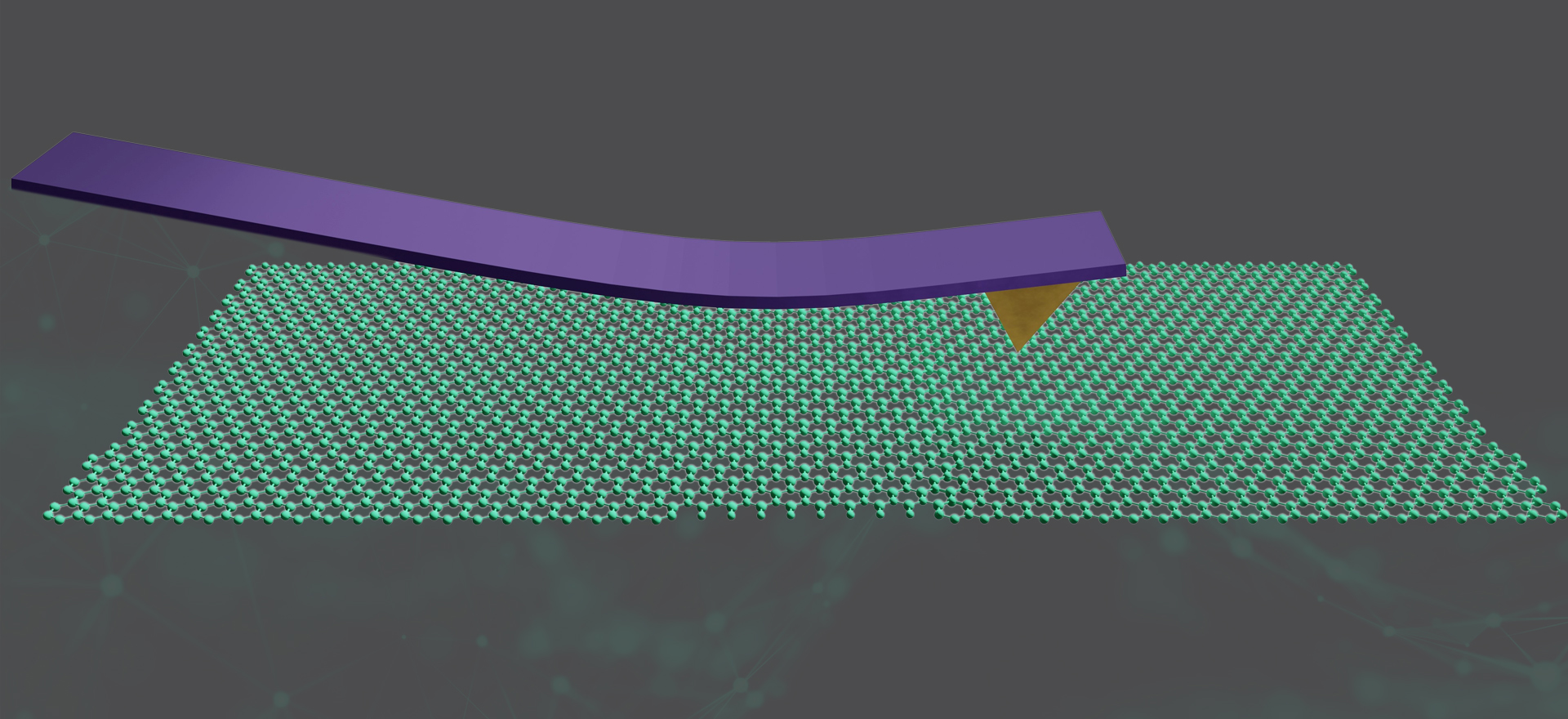
The Scanning Probe Microscope (SPM) provides high-resolution imaging of surfaces by means of a fine probe that allows not only physical images, but also surface manipulations, and measurement of mechanical, electrical, and various force-related characteristics of the surface.
SPM is a family of techniques that have in common a fine probe that physically scans across a surface while measuring not only topography, but also electrical, mechanical, magnetic, optical, and other properties at resolutions that can reach the atomic level. The SPM can be operated in any environment – ambient, vacuum, or liquid. In addition to SPM instrumentation, the lab also houses a nanoindenter for precise nanomechanical testing on a wide range of samples.
Please note the use of acronyms on these pages:
- STM: scanning tunneling microscopy
- AFM: atomic force microscopy
- EFM: electric force microscopy
- MFM: magnetic force microscopy
- SKPM: Scanning Kelvin Probe Microscopy